Release 2.9.0 (r2020-1)
Copyright © 2020 Pi Innovo
13-Apr-2020
Table of Contents
- 1. Technical specification
- 2. Connector pinout
- 3. Internal signals
- 4. Operational details
- 4.1. ECU power
- 4.2. ECU power — control
- 4.3. ECU power — wake-on-CAN
- 4.4. Analog inputs
- 4.5. Analog inputs — relationship between sensor supplies and inputs
- 4.6. Analog inputs — VREF diode inputs
- 4.7. Analog inputs — temperature, internal
- 4.8. Analog outputs
- 4.9. Digital inputs
- 4.10. Digital inputs — frequency measurement
- 4.11. Digital inputs — SENT
- 4.12. Digital outputs
- 4.13. Digital outputs — low-side
- 4.14. Digital outputs — monitors
- 4.15. Serial inputs and outputs
- 4.16. Communication — CAN
- 4.17. Communication — LIN
- 4.18. Memory — configuration
- 4.19. Memory — non-volatile storage and lifetime
- 4.20. Memory — calibration capabilities
- 4.21. System modes
- 4.22. Flash codes
- 4.23. Floating point capabilities
- 4.24. Customization — build options
- 5. Dimensions
- A. Contact information
List of Figures
- 1.1. Block diagram of M110 functionality
- 4.1. Switching arrangement for main power supply, wake-on-CAN enabled
- 4.2. VREF arrangement
- 4.3. VREF diode monitor arrangement
- 4.4. Frequency measurement
- 4.5. Switching arrangement for low-side digital outputs
- 4.6. Flash code sequence
- 5.1. Outline of physical dimensions
List of Tables
- 1.1. Specification
- 1.2. Function reference
- 2.1. Part numbers of the mating connector
- 2.2. Part numbers for the pins
- 2.3. Part numbers for harness tools
- 2.4. Connector pinout — Pocket A
- 2.5. Part numbers of the mating connector
- 2.6. Part numbers for the pins
- 2.7. Part numbers for harness tools
- 2.8. Connector pinout — Pocket B
- 3.1. Internal signals
- 4.1. Internal temperature conversion
- 4.2. Memory configurations supported
- 4.3. System mode selection
- 4.4. Flash code example
- 4.5. Flash codes
- 4.6. Floating point conditions
This document is the technical specification for OpenECU part 01T-068883-01m00. Within this document, that part is referred to as the M110-000 ECU.
Note
For a list of issues and possible work arounds for this ECU, found after publication of this document, please refer to the hardware errata for this ECU (named 29T-068432 M110 Technical Spec Errata).
Specific option control may exist for this part. In that case, parts of this document will be overridden by an option control specific technical specification. Please refer to the option control technical specification for more information.
This technical specification relates to the following ECU variant:
M110-000 — for development and testing, including full interactive calibration tool integration.
Table 1.1. Specification
| Specification | Variant |
|---|---|
| M110-000 | |
| Status | Prototype [a] |
| Processor | MPC5534 |
| Rate | 80MHz |
| Code space | 512KiB |
| RAM space | up to 64KiB [b] |
| Calibration space | up to 48KiB [b] |
| Calibratable | Y |
| Reprogrammable | Y |
| Power control relays | - |
| Actuator supplies | - |
| Sensor supplies | 1 |
| Inputs | 10 |
| Outputs | 14 |
| CAN buses | 4 |
| LIN buses | 2 |
| RS232 links | - |
| Connectors | 2x20 |
| Weight | 350g |
| Vibration | 6g random RMS |
| Shock capability | - [c] |
| Enclosure | IP65K |
| EMC | - [c] |
| Partial operating voltage | 6 to 36V |
| Full operating voltage | 9 to 32V [d] |
| Standby current (typical) | 0.45mA at 12V [e] |
| Operating current (typical) | 100mA at 12V [f] |
| Operating temperature range | -40 to +85°C |
| Storage temperature range (installation) | -40 to +85°C |
| Storage temperature range (shipping) | -40 to +85°C |
[a] Target ECU at a prototype stage, available in limited quantities. [b] See list of possible memory configurations in section 'Memory - configuration'. [c] Please contact Pi for details. [d] Designed for 12V or 24V vehicles. [e] 1.75mA at 24V. [f] 75mA at 24V. When running idle task with I/O disconnected. | |
This shows a high-level pictoral description of this ECU's capability.
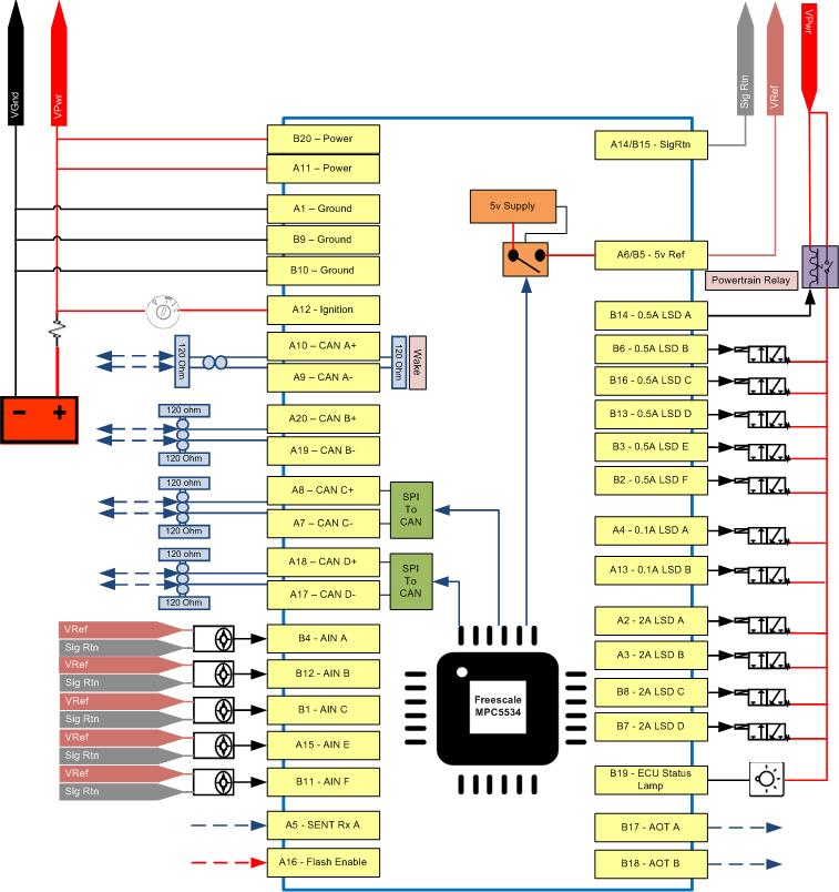
Various input and output functionality is supported where some pins may be capable of more than one function. Some functions require a combination of pins but not all pin combinations are possible.
Table 1.2. Function reference
| I/O type | External | Internal | Pins |
|---|---|---|---|
| Power | |||
| ECU supply | 1 | - | A11+B20 |
| ECU ground | 1 | - | A1+B9+B10 |
| Sensor supply | 1 | - | A6+B5 |
| Module control, status | |||
| Ignition sense | 1 | - | A12 |
| Module control FEPS | 1 | - | A16 |
| Module status Flash code | 1 | - | B19 |
| Communication | |||
| CAN buses | 4 | - | A8+A7, A10+A9, A18+A17, A20+A19 |
| LIN buses | 2 | - | A4, A13 |
| Inputs — time based | |||
| Analogue | 10 | 28 | A5, A7, A8, A15, A17, A18, B1, B4, B11, B12 |
| Digital | 11 | 17 | A5, A7, A8, A12, A15, A17, A18, B1, B4, B11, B12 |
| Frequency | 10 | 12 | A5, A7, A8, A15, A17, A18, B1, B4, B11, B12 |
| PWM | - | 12 | |
| Quadrature | - | 12 | |
| SENT | 3 | - | A5, A15, B11 |
| Outputs — time based | |||
| Analogue output | 2 | - | B17, B18 |
| Digital | 12 | 6 | A2, A3, A4, A13, B2, B3, B6, B7, B8, B13, B14, B16 |
| PWM | 12 | - | A2, A3, A4, A13, B2, B3, B6, B7, B8, B13, B14, B16 |
| PWM synchronised | 12 | - | A2, A3, A4, A13, B2, B3, B6, B7, B8, B13, B14, B16 |
| Inputs — angle based | |||
| None | - | - | |
| Outputs — angle based | |||
| None | - | - | |
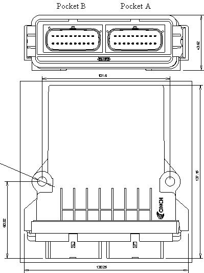
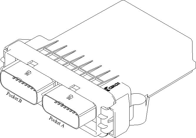
The M110-000 variants have two ECU connectors (pockets) named A and B, which have pinouts as given in the following tables. Currents listed are RMS unless otherwise stated.
The following abbreviations are used in the pinout tables below:
C Communication I Input M Monitor O Output P Power
CT Current trip GND Ground PSU Power supply PWR Power
Connector packs can be ordered from Pi. Individual connector components can be ordered from Pi or from various manufacturers.
Table 2.1. Part numbers of the mating connector
| Supplier | Part number | Color | Part |
|---|---|---|---|
| Molex | 33472-2001 | Black | Female connector |
Table 2.2. Part numbers for the pins
| Supplier | Part number | Part |
|---|---|---|
| Molex | 33012-3002 | Female terminal |
| 0343450001 | Plug for unused position |
Table 2.3. Part numbers for harness tools
| Supplier | Part number | Part |
|---|---|---|
| Molex | 0638116000 | Crimp tool |
| 63813-1500 | Extraction tool |
Table 2.4. Connector pinout — Pocket A
| Main connector — Pocket A | ||||||||
|---|---|---|---|---|---|---|---|---|
| Pin | P | Function | I/O | M | Loading | Filter | Range | Notes |
| A1 | VGND | P | 20A | Rating specified at maximum operating temperature. To achieve the current carrying capability of this pin, the maximum wire gauge allowed in the wire harness must be used. | ||||
| A2 | Digital | O | Y | 2A | Default population: Populated. Related to internal channels Monitor (d), Monitor (status) and Monitor (v). | |||
| A3 | Digital | O | Y | 2A | Default population: Populated. Related to internal channels Monitor (d), Monitor (status) and Monitor (v). | |||
| A4 | Digital | O | Y | 100mA | Default population: Populated. Related to internal channels Monitor (d) and Monitor (v). | |||
| A5 | Analogue | I | 20kR to 5V | 1.68kHz | 0V to 5V | 12-bit unsigned conversion. To convert measured voltage (Vm) to actual voltage (Va) use the equation, Va=Vm*1.056. Default population: SENTrx. | ||
| Digital | 254.41kHz | Default population: Not populated. | ||||||
| SENT | Default population: Populated. Note: SENT Rx and 0-5V AIN are both equipped for the default population. | |||||||
| A6 | Sensor supply | P | Y | 5V, 250mA | Sensor supply. Current capability listed is total for both supply pins. Can be turned on and off by the application for diagnostics purposes. Related to internal channels DOT enable and Monitor (v). | |||
| A7 | CAN- (low) | C | CAN bus C low (-ve), see also: A8. Related to internal channel DOT disable-CAN. | |||||
| Analogue | I | 51kR to GND | 1.59kHz | 0V to 15.02V | 12-bit unsigned conversion. To convert measured voltage (Vm) to actual voltage (Va) use the equation, Va=Vm*3.003. Default population: Not Populated. | |||
| Digital | 3.9kR to 5V | 0V to 5V | Default population: Not populated. | |||||
| A8 | CAN+ (high) | C | CAN bus C high (+ve), see also: A7. Related to internal channel DOT disable-CAN. | |||||
| Analogue | I | 51kR to GND | 1.59kHz | 0V to 15.02V | 12-bit unsigned conversion. To convert measured voltage (Vm) to actual voltage (Va) use the equation, Va=Vm*3.003. Default population: Not Populated. | |||
| Digital | 3.9kR to 5V | 0V to 5V | Default population: Not populated. | |||||
| A9 | CAN- (low) | C | 120R to CANA_P | CAN bus A low (-ve). Default CAN bus for reprogramming unless overridden by the application, see also: A10. Related to internal channels DOT disable-CAN and Monitor (no fault). | ||||
| A10 | CAN+ (high) | C | 120R to CANA_N | CAN bus A high (+ve). Default CAN bus for reprogramming unless overridden by the application, see also: A9. Related to internal channels DOT disable-CAN and Monitor (no fault). | ||||
| A11 | VPWR | P | 20A | Rating specified at maximum operating temperature. To achieve the current carrying capability of this pin, the maximum wire gauge allowed in the wire harness must be used. Related to internal channel AIN VPWR. | ||||
| A12 | Digital | I | 4.7kR to VGND | 100Hz | 0V to VPWR | Key position (ignition sense) input. This signal is inverted in hardware. A voltage higher than 5V worst case will wake up the ECU. Related to internal channel DOT enable-PSU-hold. | ||
| A13 | Digital | O | Y | 100mA | Default population: Populated. Related to internal channels Monitor (d) and Monitor (v). | |||
| A14 | Sensor ground | P | 250mA | Sensor ground, VRTND. | ||||
| A15 | Analogue | I | 51kR to GND | 531Hz | 0V to 5V | 12-bit unsigned conversion. Unscaled. Default population: Pulldown. | ||
| Digital | Default population: Not populated. | |||||||
| SENT | ||||||||
| A16 | FEPS | I | 92kR to 5V | -18V | Module flash programming control. | |||
| A17 | CAN- (low) | C | CAN bus D low (-ve), see also: A18. Related to internal channel DOT disable-CAN. | |||||
| Analogue | I | 51kR to GND | 1.59kHz | 0V to 15.02V | 12-bit unsigned conversion. To convert measured voltage (Vm) to actual voltage (Va) use the equation, Va=Vm*3.003. Default population: Not Populated. | |||
| Digital | 3.9kR to 5V | 0V to 5V | Default population: Not populated. | |||||
| A18 | CAN+ (high) | C | CAN bus D high (+ve), see also: A17. Related to internal channel DOT disable-CAN. | |||||
| Analogue | I | 51kR to GND | 1.59kHz | 0V to 15.02V | 12-bit unsigned conversion. To convert measured voltage (Vm) to actual voltage (Va) use the equation, Va=Vm*3.003. Default population: Not Populated. | |||
| Digital | 3.9kR to 5V | 0V to 5V | Default population: Not populated. | |||||
| A19 | CAN- (low) | C | CAN bus B low (-ve), see also: A20. Related to internal channel DOT disable-CAN. | |||||
| A20 | CAN+ (high) | C | CAN bus B high (+ve), see also: A19. Related to internal channel DOT disable-CAN. | |||||
Connector packs can be ordered from Pi. Individual connector components can be ordered from Pi or from various manufacturers.
Table 2.5. Part numbers of the mating connector
| Supplier | Part number | Color | Part |
|---|---|---|---|
| Molex | 33472-2002 | Grey | Female connector |
Table 2.6. Part numbers for the pins
| Supplier | Part number | Part |
|---|---|---|
| Molex | 33012-3002 | Female terminal |
| 0343450001 | Plug for unused position |
Table 2.7. Part numbers for harness tools
| Supplier | Part number | Part |
|---|---|---|
| Molex | 0638116000 | Crimp tool |
| 63813-1500 | Extraction tool |
Table 2.8. Connector pinout — Pocket B
| Main connector — Pocket B | ||||||||
|---|---|---|---|---|---|---|---|---|
| Pin | P | Function | I/O | M | Loading | Filter | Range | Notes |
| B1 | Analogue | I | 220R to 5V | 531Hz | 0V to 5V | 12-bit unsigned conversion. Unscaled. Default population: Pullup. Related to internal channel AIN Vref diode. | ||
| Digital | Default population: Not populated. | |||||||
| B2 | Digital | O | Y | 500mA | Default population: Populated. Related to internal channels Monitor (d) and Monitor (v). | |||
| B3 | Digital | O | Y | 500mA | Default population: Populated. Related to internal channels Monitor (d) and Monitor (v). | |||
| B4 | Analogue | I | 4.7kR to 5V | 574Hz | 0V to 416mV | 12-bit unsigned conversion. To convert measured voltage (Vm) to actual voltage (Va) use the equation, Va=Vm*0.082. Default population: RTD. Related to internal channel AIN Vref diode. | ||
| Digital | 0V to 5V | Default population: Not populated. | ||||||
| B5 | Sensor supply | P | Y | 5V, 250mA | Sensor supply. Current capability listed is total for both supply pins. Can be turned on and off by the application for diagnostics purposes. Related to internal channels DOT enable and Monitor (v). | |||
| B6 | Digital | O | Y | 500mA | Default population: Populated. Related to internal channels Monitor (d) and Monitor (v). | |||
| B7 | Digital | O | Y | 2A | Default population: Populated. Related to internal channels Monitor (d), Monitor (status) and Monitor (v). | |||
| B8 | Digital | O | Y | 2A | Default population: Populated. Related to internal channels Monitor (d), Monitor (status) and Monitor (v). | |||
| B9 | VGND | P | 20A | Rating specified at maximum operating temperature. To achieve the current carrying capability of this pin, the maximum wire gauge allowed in the wire harness must be used. | ||||
| B10 | VGND | P | 20A | Rating specified at maximum operating temperature. To achieve the current carrying capability of this pin, the maximum wire gauge allowed in the wire harness must be used. | ||||
| B11 | Analogue | I | 51kR to GND | 531Hz | 0V to 5V | 12-bit unsigned conversion. Unscaled. Default population: Pulldown. | ||
| Digital | Default population: Not populated. | |||||||
| SENT | ||||||||
| B12 | Analogue | I | 10kR to 5V | 531Hz | 0V to 5V | 12-bit unsigned conversion. Unscaled. Default population: Pullup. Related to internal channel AIN Vref diode. | ||
| Digital | Default population: Not populated. | |||||||
| B13 | Digital | O | Y | 500mA | Default population: Populated. Related to internal channels Monitor (d) and Monitor (v). | |||
| B14 | Digital | O | Y | 500mA | Default population: Populated. Related to internal channels Monitor (d) and Monitor (v). | |||
| B15 | Sensor ground | P | 250mA | Sensor ground, VRTND. | ||||
| B16 | Digital | O | Y | 500mA | Default population: Populated. Related to internal channels Monitor (d) and Monitor (v). | |||
| B17 | Analogue output | O | Y | 0 to 5V | Serial output. Related to internal channel Monitor (v). | |||
| B18 | Analogue output | O | Y | 0 to 5V | Serial output. Related to internal channel Monitor (v). | |||
| B19 | Flash code | O | Low side | 20mA | ECU status information. See section "Flash Codes" for detailed description. Default population: Populated. | |||
| B20 | VPWR | P | 20A | Rating specified at maximum operating temperature. To achieve the current carrying capability of this pin, the maximum wire gauge allowed in the wire harness must be used. Related to internal channel AIN VPWR. | ||||
Table 3.1. Internal signals
| Signal | I/O | Signal type | Range | Notes |
|---|---|---|---|---|
| Analogue | ||||
| AIN 3.3V | I | Analogue | 0V to 5V | Internal 3.3V supply monitor. 12-bit unsigned conversion. Unscaled. Default population: Populated. |
| AIN 5.0V | I | Analogue | 0V to 6.96V | Internal 5V supply monitor. 12-bit unsigned conversion. To convert measured voltage (Vm) to actual voltage (Va) use the equation, Va=Vm*1.393. Default population: Populated. |
| AIN VPWR (pin A11 and B20) | I | Analogue | 0V to 40V | 12-bit unsigned conversion. To convert measured voltage (Vm) to actual voltage (Va) use the equation, Va=Vm*8.000. Default population: Populated. |
| AIN Vref | I | Analogue | 0V to 10V | Internal Analog input reference monitor. 12-bit unsigned conversion. To convert measured voltage (Vm) to actual voltage (Va) use the equation, Va=Vm*2. Default population: Populated. |
| AIN Vref diode (pin B1) | I | Analogue | 0V to 5V | 12-bit unsigned conversion. Unscaled. Default population: Populated. |
| AIN Vref diode (pin B12) | I | Analogue | 0V to 5V | 12-bit unsigned conversion. Unscaled. Default population: Not Populated. |
| AIN Vref diode (pin B4) | I | Analogue | 0V to 5V | 12-bit unsigned conversion. Unscaled. Default population: Populated. |
| AIN VRH | I | Analogue | 0V to 5V | 12-bit unsigned conversion. 5V reference for analogue input conversions. |
| AIN VRH-VRL 25% | I | Analogue | 0V to 5V | 12-bit unsigned conversion. 1.25V reference for analogue input conversions. |
| AIN VRH-VRL 50% | I | Analogue | 0V to 5V | 12-bit unsigned conversion. 2.5V reference for analogue input conversions. Will read as 2.48V due to 20mV offset in processor implementation. |
| AIN VRH-VRL 75% | I | Analogue | 0V to 5V | 12-bit unsigned conversion. 3.75V reference for analogue input conversions. |
| AIN VRL | I | Analogue | 0V to 5V | 12-bit unsigned conversion. 0V reference for analogue input conversions. |
| Digital | ||||
| DOT enable (pin A6 and B5) | O | Digital | 0 or 1 | Set to high to enable sensor supply. Set to low to disable. |
| DOT enable-PSU-hold (pin A12) | O | Digital | 0 or 1 | Digital output controlling the power supply to ECU in conjunction with the key position (ignition sense) input. Set high to enable power hold and low to disable. |
| Monitor (d) (pin A13) | I | Digital | 0 or 1 | Output state. See section "Digital outputs - monitors" for detailed descripton. Default population: Populated. |
| Monitor (d) (pin A2) | I | Digital | 0 or 1 | Output state. See section "Digital outputs - monitors" for detailed descripton. Default population: Populated. |
| Monitor (d) (pin A3) | I | Digital | 0 or 1 | Output state. See section "Digital outputs - monitors" for detailed descripton. Default population: Populated. |
| Monitor (d) (pin A4) | I | Digital | 0 or 1 | Output state. See section "Digital outputs - monitors" for detailed descripton. Default population: Populated. |
| Monitor (d) (pin B13) | I | Digital | 0 or 1 | Output state. See section "Digital outputs - monitors" for detailed descripton. Default population: Populated. |
| Monitor (d) (pin B14) | I | Digital | 0 or 1 | Output state. See section "Digital outputs - monitors" for detailed descripton. Default population: Populated. |
| Monitor (d) (pin B16) | I | Digital | 0 or 1 | Output state. See section "Digital outputs - monitors" for detailed descripton. Default population: Populated. |
| Monitor (d) (pin B2) | I | Digital | 0 or 1 | Output state. See section "Digital outputs - monitors" for detailed descripton. Default population: Populated. |
| Monitor (d) (pin B3) | I | Digital | 0 or 1 | Output state. See section "Digital outputs - monitors" for detailed descripton. Default population: Populated. |
| Monitor (d) (pin B6) | I | Digital | 0 or 1 | Output state. See section "Digital outputs - monitors" for detailed descripton. Default population: Populated. |
| Monitor (d) (pin B7) | I | Digital | 0 or 1 | Output state. See section "Digital outputs - monitors" for detailed descripton. Default population: Populated. |
| Monitor (d) (pin B8) | I | Digital | 0 or 1 | Output state. See section "Digital outputs - monitors" for detailed descripton. Default population: Populated. |
| Monitor (status) (pin A2) | I | Digital | 0 or 1 | Low-side driver status. Low indicates fault. See section "Digital outputs - monitors" for detailed descripton. |
| Monitor (status) (pin A3) | I | Digital | 0 or 1 | Low-side driver status. Low indicates fault. See section "Digital outputs - monitors" for detailed descripton. |
| Monitor (status) (pin B7) | I | Digital | 0 or 1 | Low-side driver status. Low indicates fault. See section "Digital outputs - monitors" for detailed descripton. |
| Monitor (status) (pin B8) | I | Digital | 0 or 1 | Low-side driver status. Low indicates fault. See section "Digital outputs - monitors" for detailed descripton. |
| Digital (CAN) | ||||
| DOT disable-CAN (pin A10 and A9) | O | Digital | 0 or 1 | Digital output controlling CAN transmission. Set high to disable transmission, low to enable. |
| DOT disable-CAN (pin A18 and A17) | O | Digital | 0 or 1 | Digital output controlling CAN transmission. Set high to disable transmission, low to enable. |
| DOT disable-CAN (pin A20 and A19) | O | Digital | 0 or 1 | Digital output controlling CAN transmission. Set high to disable transmission, low to enable. |
| DOT disable-CAN (pin A8 and A7) | O | Digital | 0 or 1 | Digital output controlling CAN transmission. Set high to disable transmission, low to enable. |
| Monitor (no fault) (pin A10 and A9) | I | Digital | 0 or 1 | Digital input indicating an error with CAN A (active low). |
| Memory check | ||||
| Monitor (counter eTPU background task) | I | Digital data | 0 to 65535 | Cyclic counter providing number of times the eTPU background task runs. Its rate of increase can be used to determine the rate of the background task. |
| Monitor (fc SDM-checksum) | I | Digital data | 0 to 65535 | Saturating counter providing number of times the eTPU module's data memory failed a checksum test. |
| Temperature monitor | ||||
| AIN PCB temp | I | Analogue | -40°C to +125°C | Internal ECU temperature measurement. 12-bit unsigned conversion. Conversion from voltage to temperature is non-linear and specified by a look-up table. Default population: Populated. |
| Voltage monitor | ||||
| Monitor (v) (pin A13) | I | Analogue | 0V to 6.1V | 12-bit unsigned conversion. To convert measured voltage (Vm) to actual voltage (Va) use the equation, Va=Vm*1.220. Default population: Not Populated. |
| Monitor (v) (pin A2) | I | Analogue | 0V to 6.1V | 12-bit unsigned conversion. To convert measured voltage (Vm) to actual voltage (Va) use the equation, Va=Vm*1.220. Default population: Not Populated. |
| Monitor (v) (pin A3) | I | Analogue | 0V to 6.1V | 12-bit unsigned conversion. To convert measured voltage (Vm) to actual voltage (Va) use the equation, Va=Vm*1.220. Default population: Not Populated. |
| Monitor (v) (pin A4) | I | Analogue | 0V to 6.1V | 12-bit unsigned conversion. To convert measured voltage (Vm) to actual voltage (Va) use the equation, Va=Vm*1.220. Default population: Not Populated. |
| Monitor (v) (pin A6 and B5) | I | Analogue | 0V to 5.71V | 12-bit unsigned conversion. To convert measured voltage (Vm) to actual voltage (Va) use the equation, Va=Vm*1.143. Default population: Populated. |
| Monitor (v) (pin B13) | I | Analogue | 0V to 6.1V | 12-bit unsigned conversion. To convert measured voltage (Vm) to actual voltage (Va) use the equation, Va=Vm*1.220. Default population: Not Populated. |
| Monitor (v) (pin B14) | I | Analogue | 0V to 6.1V | 12-bit unsigned conversion. To convert measured voltage (Vm) to actual voltage (Va) use the equation, Va=Vm*1.220. Default population: Not Populated. |
| Monitor (v) (pin B16) | I | Analogue | 0V to 6.1V | 12-bit unsigned conversion. To convert measured voltage (Vm) to actual voltage (Va) use the equation, Va=Vm*1.220. Default population: Not Populated. |
| Monitor (v) (pin B17) | I | Analogue | 0V to 15.02V | 12-bit unsigned conversion. To convert measured voltage (Vm) to actual voltage (Va) use the equation, Va=Vm*3.003. Default population: Populated. |
| Monitor (v) (pin B18) | I | Analogue | 0V to 15.02V | 12-bit unsigned conversion. To convert measured voltage (Vm) to actual voltage (Va) use the equation, Va=Vm*3.003. Default population: Populated. |
| Monitor (v) (pin B2) | I | Analogue | 0V to 6.1V | 12-bit unsigned conversion. To convert measured voltage (Vm) to actual voltage (Va) use the equation, Va=Vm*1.220. Default population: Not Populated. |
| Monitor (v) (pin B3) | I | Analogue | 0V to 6.1V | 12-bit unsigned conversion. To convert measured voltage (Vm) to actual voltage (Va) use the equation, Va=Vm*1.220. Default population: Not Populated. |
| Monitor (v) (pin B6) | I | Analogue | 0V to 6.1V | 12-bit unsigned conversion. To convert measured voltage (Vm) to actual voltage (Va) use the equation, Va=Vm*1.220. Default population: Not Populated. |
| Monitor (v) (pin B7) | I | Analogue | 0V to 6.1V | 12-bit unsigned conversion. To convert measured voltage (Vm) to actual voltage (Va) use the equation, Va=Vm*1.220. Default population: Not Populated. |
| Monitor (v) (pin B8) | I | Analogue | 0V to 6.1V | 12-bit unsigned conversion. To convert measured voltage (Vm) to actual voltage (Va) use the equation, Va=Vm*1.220. Default population: Not Populated. |
- 4.1. ECU power
- 4.2. ECU power — control
- 4.3. ECU power — wake-on-CAN
- 4.4. Analog inputs
- 4.5. Analog inputs — relationship between sensor supplies and inputs
- 4.6. Analog inputs — VREF diode inputs
- 4.7. Analog inputs — temperature, internal
- 4.8. Analog outputs
- 4.9. Digital inputs
- 4.10. Digital inputs — frequency measurement
- 4.11. Digital inputs — SENT
- 4.12. Digital outputs
- 4.13. Digital outputs — low-side
- 4.14. Digital outputs — monitors
- 4.15. Serial inputs and outputs
- 4.16. Communication — CAN
- 4.17. Communication — LIN
- 4.18. Memory — configuration
- 4.19. Memory — non-volatile storage and lifetime
- 4.20. Memory — calibration capabilities
- 4.21. System modes
- 4.22. Flash codes
- 4.23. Floating point capabilities
- 4.24. Customization — build options
The power supply pins (VPWR A11+B20) and the ground pins (VGND A1+B9+B10) are both rated to 20A.
The ECU VGND (pins A1+B9+B10) and sensor ground (pins A14+B15) are directly connected together via a ground plane in the ECU PCB.
The ECU is designed for 12V or 24V vehicles, with various modes of operation based on the voltage (see Table 1.1, “Specification”). The ECU is protected against reverse supply connection. All inputs and outputs are protected against short-to-VPWR or short-to-VGND over normal operating range.
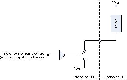
The ECU power arrangement is shown in Figure 4.1, “Switching arrangement for main power supply, wake-on-CAN enabled”.
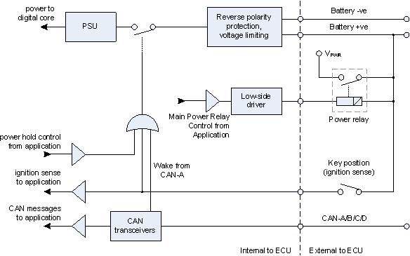
The default build option supports an ignition switch. The ECU powers up when the power supply pins (VPWR A11+B20) and key position (ignition sense) input (pin A12) are asserted. The key position voltage threshold, above which the power supply turns on, is nominally 4.0V (worst case, a minimum of 3.4V and a maximum of 4.8V). The key position (pin A12) can be read as a digital input. The application must debounce the digital input over 200 milliseconds to achieve an accurate reading.
The default build option supports wake-on-CAN. The ECU powers up when the power supply pins are asserted and the ECU receives a message on a wake-on-CAN-enabled CAN bus (see Section 4.3, “ECU power — wake-on-CAN” for more). To fully disable wake-on-CAN, ECUs can be modified with a build option.
The ECU application software can hold power to the ECU after the conditions to power up the ECU no longer exist (e.g., the ignition sense is deasserted or CAN messages are no longer present). This allows, for example, the application to complete non-volatile memory processing. For the ECU to hold power the internal DOT enable-PSU-hold channel needs to be asserted. Setting this internal channel high will hold power when the key position input is opened, setting it low will allow the ECU to power off when the key position input is opened.
Note
The ECU will turn on and assert power hold before the application starts to run. The application must disable power hold by deasserting the internal channel DOT enable-PSU-hold when the conditions to shutdown are satisfied (for instance, the ignition sense input is off and information to store in non-volatile information has been written).
One CAN bus (pins A9 and A10) provides wake-on-CAN functionality. When the ECU power is controlled using CAN messages, the ECU powers up (or wakes) when the ECU senses two bus dominant states of at most 5 microseconds, with the first dominant state followed by a recessive state of at most 5 microseconds (provided the complete dominant-recessive-dominant pattern is completed within at most 2 milliseconds). Generally this pattern is fulfilled by sending a valid CAN message.
When ECU is powered via wake-on-CAN, it is the responsibility of the application to determine how long the ECU should remain on. In order to guarantee that the application is able to run after a wake-on-CAN event, it is recommended that the application initialize the DOT enable-PSU-hold channel to high to keep the ECU powered.
When the application has completed its desired tasks, the internal digital output DOT enable-PSU-hold should be set to low to allow the ECU to shut down. Once both the power-hold output and ignition input are deasserted, the platform will disable the CAN transceivers to cause the ECU to shut down.
Note
If the ECU is initially powered via wake-on-CAN and then the ignition input becomes active while the application is running, the ECU will remain on while the ignition is on even if the power-hold is disabled.
Note
The ECU does not fully support reprogramming via wake-on-CAN, i.e. reprogramming with no ignition input. Normally if this is attempted, the ECU will power off shortly after reprogramming is initiated. However, it is possible to keep the ECU powered on and reprogram it successfully if a sufficient stream of CAN messages is maintained on one of the wake-on-CAN channels.
The analog inputs (pins A5, A7, A8, A15, A17, A18, B1, B4, B11 and B12) sample voltage with varying resolution and range. See the pin information for more details. Some of the analog inputs have additional characteristics or may not be populated by default, as detailed in the following sections.
The ECU sensor supply arrangement is shown in Figure 4.2, “VREF arrangement”. The figure shows the relationship between the internal 5V reference supply and ground, the external sensor supply and ground, and the analog inputs.
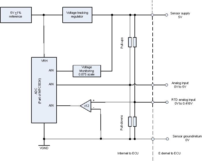
The internal precision 5V reference supplies the reference pin on the ADC. The exact sensor voltage being produced can be monitored on a (scaled) ADC channel. The scaling is detailed in Table 3.1, “Internal signals” and can be used to detect a short to battery or ground. The sensor ground is a nominal 0V.
The exact voltage on analog input pins can be read on a direct (unscaled) or an indirect (scaled) ADC channel. Standard 0-5V inputs are passed directly to the ADC with no scaling.
Some analog input pins are internally pulled up to the sensor power supply (pin A6+B5). If the sensor supply is not enabled, floating inputs will fluctuate when read by the ADC. The sensor supply must be enabled for resistance measurements made on any of these channels.
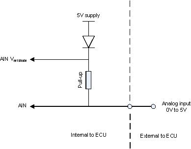
The analog inputs (B1, B4 and B12) have associated diode reference input channels that are used to monitor the voltage drop across the pull-up diodes at the pull-up resistor. These monitors can be used for more accurate measurements on their associated channels. Figure 4.3, “VREF diode monitor arrangement” shows the relationship between the 5V supply, the analog input and the diode reference.
The ECU has an internal thermistor temperature sensor. The conversion from input voltage, VADC, to temperature, TSENSOR, is non-linear. Table 4.1, “Internal temperature conversion” provides nominal, median values; the minimum and maximum are within ±10% from -40°C and up, and ±5% above 95°C.
Table 4.1. Internal temperature conversion
| TSENSOR °C | VADC V | TSENSOR °C | VADC V |
|---|---|---|---|
| -40 | 0.144484 | 45 | 3.480803 |
| -35 | 0.198075 | 50 | 3.676984 |
| -30 | 0.267652 | 55 | 3.851516 |
| -25 | 0.356328 | 60 | 4.005223 |
| -20 | 0.467202 | 65 | 4.139518 |
| -15 | 0.602969 | 70 | 4.256080 |
| -10 | 0.765533 | 75 | 4.356805 |
| -5 | 0.955566 | 80 | 4.443536 |
| 0 | 1.172141 | 85 | 4.518059 |
| 5 | 1.412429 | 90 | 4.581998 |
| 10 | 1.671849 | 95 | 4.636847 |
| 15 | 1.944315 | 100 | 4.683893 |
| 20 | 2.222815 | 105 | 4.724277 |
| 25 | 2.500000 | 110 | 4.758972 |
| 30 | 2.769285 | 115 | 4.788823 |
| 35 | 3.025023 | 120 | 4.814544 |
| 40 | 3.263090 | 125 | 4.836750 |
The analog outputs (pins B17 and B18) drive a constant voltage into an external
load. See the Sim-API pax_AnalogOutput block and C-API
pax_dac_output() function.
The valid range of the output is between 0.5V and 4.5V. The application can detect short-to-ground and short-to-battery faults by checking if the corresponding voltage monitor indicates it is out of the valid range.
The digital inputs (pins A5, A7, A8, A15, A17, A18, B1, B4, B11 and B12) sample a digital state, allowing the measurement of switches or pulsing inputs. See the pin information for more details. Some of the digital inputs have additional characteristics or may not be populated by default, as detailed in the following sections.
These digital inputs are not popuated by default. To support a variety of sensors, the ECU is pre-populated with a default selection of inputs with varying voltage thresholds and pull strengths. The inputs are not inverted.
See Chapter 2, Connector pinout for more information. In some cases the default selection will not meet the requirements of all customers. To help, Pi can modify the ECU PCB component population to adjust these characteristics as build options. Contact Pi for further information.
Note
The external signals are all low pass filtered to prevent signals of excessive frequency from tying up the target processor.
The ECU measures a signal frequency and duty cycle by capturing the time of the signal's filtered digital edges arriving at the processor. The time between similar edges gives the cycle period of the signal, and the inverse of the cycle period gives the frequency of the signal. The time between opposing edges gives the on and off periods, and the ratio of either the on or off period to the cycle period gives the corresponding on or off duty cycle.
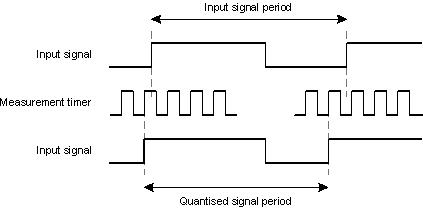
The filtered digital edges for each input pin are captured relative to a digital timer. The digital timer has two properties that affect the measurable range of frequency.
- Timer frequency
Each timer counts at a fixed frequency. When the state of the filtered digital signal changes (an edge occurs), the timer count is captured. If the state of the filtered digital signal changes between timer counts, then the measured frequency is quantised and less accurate. The resolution of the measured frequency can be calculated as:
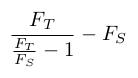
where FT is the timer frequency and FS is the signal frequency.
Note that as the signal frequency increases, the measured resolution decreases. For instance, with a 1000 Hz input signal and 4 MHz timer, results in a resolution of approximately 0.25 Hz. A 10000 Hz input signal and 4 MHz time, results in a resolution of appoximately 25 Hz.
Pins A5, A7, A8, A15, A17, A18, B1, B4, B11 and B12 use a 4MHz timer for frequency inputs.
Pins A2, A3, A4, A13, B2, B3, B6, B7, B8, B13, B14 and B16 have digtial state monitors which also can use a 4MHz timer for frequency measurement.
- Timer size
Each timer is free running, meaning the timer is incremented modulo N, where N is the size of the timer. The larger N, the longer a signal cycle period that can be measured. Thus the size of the timer limits the lowest frequency that can be measured. The user guide documentation indicates measurement frequency ranges.
Pins A5, A15 and B11 provide support for SENT sensors. To use the SENT channels, see the C-API or Sim-API User Guide for further details.
The digital outputs (pins A2, A3, A4, A13, B2, B3, B6, B7, B8, B13, B14 and B16) are a collection of low-side drivers, and are described in further detail in the following section.
With the low-side outputs (pins A2, A3, A4, A13, B2, B3, B6, B7, B8, B13, B14 and B16) the ECU switches the output pin to ground, the actuator is connected to the output pin and to VPWR.
The low-side output pins are protected against over-voltage up to 40V. These outputs can drive resistive loads at a maximum rate of 10 kHz.
The low-side digital outputs contain a mixture of monitoring circuitry that provides unconditioned diagnostic information that can be used for electrical diagnostics, such as state, voltage, and status monitors. These monitors are available to the application as individual analog or digital inputs.
Drive state — digital output state monitors are provided for pins A2, A3, A4, A13, B2, B3, B6, B7, B8, B13, B14 and B16. Drive state monitors provide the driven state, on or off, of an output pin or an internal function of the ECU. They can also be read as frequency input to measure the driven frequecy as described in Section 4.10, “Digital inputs — frequency measurement”.
Voltage — voltage monitors are provided for pins A2, A3, A4, A6+B5, A13, B2, B3, B6, B7, B8, B13, B14, B16, B17 and B18. The monitors provide a voltage reading of power supply and digital output circuits.
Status — status monitors are provided for pins A2, A3, B7 and B8. The status monitors indicate overtemperature and output openload OFF-state low voltage conditions.
The status monitor is normally pulled high, but will be pulled low when:
The low-side FET is overtemperature and the input is commanded on.
The low-side FET input is commanded off and the drain (output) is less than a threshold between 1.7V max or 0.6V min (1.2V nominal).
These monitors can be used by the application to determine electrical faults. For instance, if a digital output is turned on but the corresponding state monitor reads off, then there is likely a short or open in the circuit.
Some of the internal and external inputs and outputs are classed as serial. The connector pinout tables and internal channel tables above specify whether a pin or channel is serial or not.
When a serial input is read, the measurement reflects the value of the input taken last time the application task ended. I.e., the value of the input is delayed by one cycle of the task period. When a serial output is set, the driven state is updated at the end of the current application task. I.e., there is a delay between requesting a change in the output state, and the output state honoring that request.
The CAN buses (pins A8+A7, A10+A9, A18+A17 and A20+A19) are implemented using high-speed CAN transceivers, compatible with J1939. The default CAN bus (pins A10+A9) has a terminating resistor fitted; the other CAN buses require external termination, by defualt.
One CAN bus (pins A9 and A10) has wake-on-CAN functionality (see Section 4.3, “ECU power — wake-on-CAN” for more details).
Note
Some CAN busses (pins A7, A8, A17 and A18) are driven by an ASIC internal to the ECU which has limited functionality. Currently, these busses do not support CCP, J1939 or ISO Diagnostics.
The M110 is designed to support LIN communications. However, this option is not yet supported. Contact Pi for further information.
The ECU supports different memory configurations for application, calibration and RAM sizes (see Section 4.20, “Memory — calibration capabilities”).
Table 4.2. Memory configurations supported
| Configuration | App size (KiB) | Cal size (KiB) | RAM size (KiB) | External RAM required? | Run-time calibration supported? |
|---|---|---|---|---|---|
| A [a] | 512 | 32 | 32 | N | Y |
| B | 512 | 48 | 16 | N | Y |
| C | 512 | 16 | 48 | N | Y |
| D | 512 | 256 | 64 | N | N |
[a] If an OpenECU target that supports memory configuration is loaded with an application in which no such configuration has been specified, then configuration A will be used as the default. | |||||
The ECU supports non-volatile memory storage in Flash. Battery backed RAM is not supported.
The processor's Flash memory is split into small and large memory blocks. The application and calibration are stored in large blocks, whilst DTC information, freeze frames and so on are stored in small blocks.
The largest Flash block can take up to approximately 7.5 seconds to erase. This occurs in an environment where the Flash has been erased and programmed many times at its temperature extreme. The typical erase time is smaller, especially at ambient temperatures. Reprogramming an ECU (where many large blocks would be erased), or storing DTC information across power cycles, can therefore take some time. Users and applications should take this into consideration.
The minimum number of erase cycles is approximately 1,000 for large Flash blocks and 100,000 for small Flash blocks. This occurs in an environment where the Flash has been erased and programmed many times at its temperature extreme. The typical number of erase cycles is larger, especially at ambient temperatures.
The minimum data retention is approximately 5 years for blocks which have been erased less than 100,000 times, and approximately 20 years for blocks which have been erased less than 1,000 times.
The information about the Flash has been taken from Freescale's MPC5534 Microcontroller Data Sheet document, revision 4 (dated Mar 2008).
The ECU supports both offline calibration (where all of the ECU's calibration memory is reprogrammed whilst the application is stopped) and online calibration (where individual calibrations can be modified whilst the application runs). These calibration capabilities are supported through the meomory configurations listed above:
The ECU can run in one of two system modes: reprogramming mode and application mode. In reprogramming mode, the ECU can be reprogrammed with application software from a calibration tool. In application mode, the ECU runs the programmed application software. The ECU selects which mode to enter when it is powered up by measuring the external FEPS A16 pin.
Table 4.3. System mode selection
| FEPS (A16) Voltage | System mode |
|---|---|
| < -18V | Enter reprogramming mode. Use the default CCP settings. |
| Otherwise | Enter application mode if valid application software has previously been programmed, otherwise enter reprogramming mode. |
Note
When reprogramming an M110 over CAN ensure that the unit is operating safely within the specified operating limits. Care should be taken to not reprogram at the specified extremes of temperature or voltage.
The ECU has a dedicated external pin (pin B19) for flashing a lamp. The LED should be connected between VPWR (pin A11+B20) and pin B19.
Note
Pin B19 presents approximately 570 Ohms plus a diode drop (totalling from 0.5V to 1.4V) to ground in the on state and will typically sink 20mA when connected to an LED to VPWR; it is not capable of lighting a bulb.
The flash sequence represents a set of codes. Each code is a three digit number, where each digit is flashed a number of times equal to its value. An example would be the flash sequence for code 113. The flash sequence is broken down into a series of marks, or on and off pulses as follows:
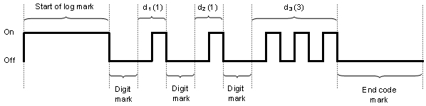
Each of the marks lasts for a specific duration:
Table 4.4. Flash code example
| Mark | Duration and meaning |
|---|---|
| Start of log mark | 3s — marks the start of the flash code list |
| Digit mark | 1s — marks the start of a digit |
| dn | ns — n digits, where the output is turned OFF for 0.5 second, then ON for 0.5 seconds, n times |
| End code mark | 3s — marks the end of a code (i.e., end of 3 digits) |
After the end code mark, the ECU will either flash the next code, or return to the start of the list and flash the first code. The ECU always has at least one code to flash.
Each code represents information about the ECU state. If there is no flash sequence, or a malformed flash sequence, then the ECU is malfunctioning. Otherwise, the flash sequence will represent one of the following codes:
Table 4.5. Flash codes
| Code | Meaning |
|---|---|
| 111 | In application mode — no other condition has been detected. |
| 112 | In reprogramming mode with the FEPS pin negative. |
| 113 | In reprogramming mode with the FEPS pin high. |
| 114 | In reprogramming mode via a FEPS-less reprogramming request. |
| 115 | In reprogramming mode because no valid application software exists. |
| 116 | In reprogramming mode due to FEPS pin electrical failure. |
| 117 | In reprogramming mode due to repeated reset during application mode. |
| 118 | In reprogramming mode due to failed application checksum tests. |
| 128 | In reprogramming mode due to failed memory check tests. |
| 119 | In reprogramming mode due to a FEPS-less ISO reprogramming request. |
| 121 | In reprogramming mode due to an unknown failure. |
| 123 | In reprogramming mode due to a watchdog reset. |
| 222 | In reprogramming mode due to the application not having a valid license. |
The ECU closely adheres to the IEEE-754 for floating point numbers.
When using Simulink, floating point Simulink models are supported — all calculations are performed using single-precision (even if the model uses double-precision, the ECU performs calculations using single-precision).
When using the C-API, floating point applications are supported — all calculations are performed using single or double precision, as determined by the application code (although double precision will incur some software overhead — see the compiler reference manual for further details).
The rounding mode is set to round-to-nearest. In some conditions, the ECU will not adhere to the IEEE-754 standard:
Table 4.6. Floating point conditions
| Condition | Result |
|---|---|
| Underflow | The result of a calculation underflow is ±0. The sign is based on the signs of the operands. |
| Overflow | The result of a calculation overflow is ±max where max is approximately 3.4 × 1038. The sign is based on the signs of the operands. |
| Divide by zero |
The ECU does not generate ±Inf, NaN or a denormalised number as the result of a calculation.
To support a variety of sensors and actuators, the ECU is pre-populated with a default selection of components with varying voltage range, pull strengths, filtering and other characteristics. In some cases the default component selection will not meet the requirements of all customers. Within design constraints, Pi can modify the ECU components to adjust these characteristics as build options. Contact Pi for further information.
The ECU has the following mechanical dimensions (mm):
If you have questions, or are experiencing issues with OpenECU please see the FAQ website:
- website
If you still have questions after searching through the FAQ, or want to discuss sales or proposals, you can contact main office:
- Tel
- +1 734 656 0140
- Fax
- +1 734 656 0141
during normal working hours (Mon to Fri, 0930 to 1700 EST).