Release 2.9.0 (r2020-1)
Copyright © 2020 Pi Innovo
13-Apr-2020
Table of Contents
- 1. Technical specification
- 2. Connector pinout
- 3. Internal signals
- 4. Operational details
- 4.1. ECU power
- 4.2. ECU power — power consumption and heat dissipation
- 4.3. ECU power — control
- 4.4. ECU power — wake-on-CAN
- 4.5. ECU power — actuator supply
- 4.6. ECU power — actuator supply monitors
- 4.7. ECU power — sensor supply
- 4.8. ECU power — sensor supply protection
- 4.9. ECU power — sensor supply monitors
- 4.10. Analogue inputs
- 4.11. Analogue inputs — relationship between sensor supplies and inputs
- 4.12. Analogue inputs — ratiometric measurement
- 4.13. Analogue inputs — temperature, RTD
- 4.14. Analogue inputs — temperature, thermistor
- 4.15. Analogue inputs — temperature, internal
- 4.16. Analogue inputs — pedal and throttle position
- 4.17. Analogue inputs — crank, VR
- 4.18. Analogue inputs — knock
- 4.19. Analogue inputs — multiplexing
- 4.20. Analogue outputs
- 4.21. Analogue outputs — constant current (switching)
- 4.22. Digital inputs
- 4.23. Digital inputs — crank and cam, Hall-effect
- 4.24. Digital inputs — frequency measurement
- 4.25. Digital inputs — quadrature
- 4.26. Digital inputs — SENT
- 4.27. Digital outputs
- 4.28. Digital outputs — low-side
- 4.29. Digital outputs — high-side
- 4.30. Digital outputs — high-side to low-side assocations
- 4.31. Digital outputs — leakage current
- 4.32. Digital outputs — monitors (unconditioned)
- 4.33. Digital outputs — monitors (conditioned)
- 4.34. Digital outputs — driver over-current protection
- 4.35. Digital outputs — waveform control
- 4.36. Digital outputs — injection variants
- 4.37. Digital outputs — injection
- 4.38. Digital outputs — injection driver protection
- 4.39. Digital outputs — injection monitors
- 4.40. Digital outputs — injection variant, M670N
- 4.41. Digital outputs — injection variant, M670S
- 4.42. Digital outputs — ignition
- 4.43. Digital outputs — ignition driver protection
- 4.44. Digital outputs — ignition monitors
- 4.45. Digital outputs — driver over-current protection
- 4.46. H-bridge outputs
- 4.47. H-bridge outputs — half-bridge operation
- 4.48. H-bridge outputs — monitors
- 4.49. H-bridge outputs — driver protection
- 4.50. Oxygen sensing
- 4.51. Oxygen sensing — narrow band HEGO
- 4.52. Oxygen sensing — wide band UEGO
- 4.53. Oxygen sensing — wide band UEGO monitors
- 4.54. Secondary processor
- 4.55. Secondary processor — E-Gas monitoring concept
- 4.56. Serial inputs and outputs
- 4.57. Communication — CAN
- 4.58. Communication — LIN
- 4.59. Communication — FlexRay
- 4.60. Memory — configuration
- 4.61. Memory — non-volatile storage and lifetime
- 4.62. Memory — calibration capabilities
- 4.63. Memory — calibration interfaces
- 4.64. System modes
- 4.65. Flash codes
- 4.66. Floating point capabilities
- 4.67. Input/output schematics
- 4.68. Customization — build options
- 4.69. Customization — daughter board options
- 5. Dimensions
- A. Contact information
List of Figures
- 4.1. Switching arrangement for main power supply, wake-on-CAN enabled
- 4.2. Switching arrangement for main power supply, wake-on-CAN partially disabled
- 4.3. Sensor supply
- 4.4. VREF arrangement
- 4.5. Knock signal processing for the HIP901x family of processors
- 4.6. Switching arrangement for constant current outputs
- 4.7. Control diagram for constant current outputs
- 4.8. Dither waveform for constant current outputs
- 4.9. Frequency measurement
- 4.10. Switching arrangement for low-side digital outputs
- 4.11. Switching arrangement for high-side digital outputs
- 4.12. Short-to-battery diagnostics for low-side digital outputs
- 4.13. Short-to-ground diagnostics for low-side digital outputs
- 4.14. Open-load gate-off diagnostics for low-side digital outputs
- 4.15. Open-load gate-on diagnostics for low-side digital outputs
- 4.16. Three stage, boosted
- 4.17. Two stage, boosted
- 4.18. Three stage, boosted, pre-energise
- 4.19. Three stage, boosted, immediate switch
- 4.20. Two stage, no boost
- 4.21. One stage, no boost
- 4.22. Injector boosted peak and hold bank diagram
- 4.23. Injector non-boosted peak and hold bank diagram
- 4.24. H-bridge arrangement
- 4.25. Connection for UEGO sensors
- 4.26. Primary and secondary processor arrangement
- 4.27. E-Gas monitoring concept
- 4.28. Flash code sequence
- 5.1. Outline of physical dimensions
List of Tables
- 1.1. Specification
- 1.2. Function reference
- 2.1. Part numbers of the mating connector
- 2.2. Part numbers for the 1.5 mm pin
- 2.3. Part numbers for the 0.635 mm pin
- 2.4. Part numbers of the pin crimp tools
- 2.5. Part numbers of the pin extraction tools
- 2.6. Connector pinout — Bay X
- 2.7. Part numbers of the mating connector
- 2.8. Part numbers for the 2.8 mm pin
- 2.9. Part numbers for the 1.5 mm pin
- 2.10. Part numbers for the 0.635 mm pin
- 2.11. Part numbers of the pin crimp tools
- 2.12. Part numbers of the pin extraction tools
- 2.13. Connector pinout — Bay Y
- 2.14. Part numbers of the mating connector
- 2.15. Part numbers for the 2.8 mm pin
- 2.16. Part numbers for the 1.5 mm pin
- 2.17. Part numbers for the 0.635 mm pin
- 2.18. Part numbers of the pin crimp tools
- 2.19. Part numbers of the pin extraction tools
- 2.20. Connector pinout — Bay Z
- 3.1. Internal signals
- 4.1. Functionality based on nominal battery voltage
- 4.2. Constant operation duty cycle for actuators
- 4.3. Sensor supply monitor voltages
- 4.4. Association of sensor supplies and analogue inputs
- 4.5. RTD temperature conversion
- 4.6. Internal temperature conversion
- 4.7. VR input voltage range
- 4.8. Required high-side to low-side association
- 4.9. Digital output leakage current (room temperature)
- 4.10. Differences between the M670B, M670N and M670S variants
- 4.11. Recommended rise-time thresholds with load
- 4.12. H-bridge disallowed frequencies
- 4.13. UEGO sensor pin connections
- 4.14. Secondary processor connector pin access
- 4.15. Secondary processor internal signal access
- 4.16. Memory configurations supported
- 4.17. System mode selection
- 4.18. Flash code example
- 4.19. Flash codes
- 4.20. Floating point conditions
This document is the technical specification for the following OpenECU parts:
| ECU | Build option |
|---|---|
|
M670B
01T-068787-04M00-000 | Non-overlapping boosted peak and hold solenoid injectors |
|
M670N
01T-068803-04M00-000 | Overlapping non-boosted peak and hold solenoid injectors |
|
M670S
01T-068850-04M00-000 | Overlapping saturating solenoid injectors |
Specific option control may exist for these parts. In that case, sections of this document will be overridden by an option control specific technical specification. Please refer to the option control technical specification for more information.
Note
For a list of known issues and work arounds for this ECU, found after publication of this document, please refer to the hardware errata for this ECU (named 29T-068787ER-xE M670 Technical Spec Errata).
The OpenECU M670 is a versatile, high performance electronic control module designed for multi-cylinder (up to 8) engine management. There are three main varieties of the M670 ECU but others are possible through build options.
The design and architecture allow the ECU to be agnostic to fuel type (diesel, gasoline, natural-gas, heavy-fuel, dual fuel), fuel injection type (PFI, GDI, CRDI) and engine combustion cycle type (CI, SI, spark-assisted CI).
The M670 supports a range of automotive sensors and actuators required for precise engine management to meet the latest emissions standards including Euro V and Tier 4. This includes support for advanced EGR and aftertreatment controls.
In addition to the standard I/O, this powerful engine control module has hardware support for the following advanced features that are critical to modern day engine controls:
- Multiple injections per stroke
- Software configurable injector current profiles
- Software configurable injector boost power supply
- Dual intake and dual exhaust cam-shaft VVT control
- Measurement of inputs in the time and angular domains
- Precision constant current outputs
- E-GAS monitoring architecture for safety including secondary microprocessor
Some functionality of the M670 can be adjusted by changing the PCB population, changing the enclosure and designing daughter cards.
- Analogue and digital Pull up/down selection
- Fuel cooled (for higher power or temperature operation)
- LIN communications daughter board
- FlexRay communications daughter board
- Analogue output daughter board
Typical applications include:
- Stand alone engine control — heavy duty and light duty
- Diesel after-treatment controller for DOC-DPF and Urea-SCR applications
- Engine plus hybrid supervisory controller in one module
- Stand-alone hybrid supervisory controller
- Stationary power engine controller
- Automatic transmission control
- Non-Powertrain applications
- Vehicle stability controller (ABS, TCS, ESC)
- Active chassis controller (Suspension, Ride Height)
- Advanced vehicle control and automation
This technical specification relates to the following ECU variants:
M670B-000 (01T-068787) — for development and testing, including full interactive calibration tool integration;
M670N-000 (01T-068803) — for development and testing, including full interactive calibration tool integration;
M670S-000 (01T-068850) — for development and testing, including full interactive calibration tool integration.
Table 1.1. Specification
| Specification | Variant | ||
|---|---|---|---|
| M670B-000 | M670N-000 | M670S-000 | |
| Status | Available [a] | Available [a] | Available [a] |
| Processor | MPC5674F | MPC5674F | MPC5674F |
| Rate | 264MHz | 264MHz | 264MHz |
| Code space | up to 3MiB [b] | up to 3MiB [b] | up to 3MiB [b] |
| RAM space | up to 256KiB [b] | up to 256KiB [b] | up to 256KiB [b] |
| Calibration space | up to 512KiB [b] | up to 512KiB [b] | up to 512KiB [b] |
| Calibratable | Y | Y | Y |
| Reprogrammable | Y | Y | Y |
| Power control relays | 1 | 1 | 1 |
| Actuator supplies | 4 | 4 | 4 |
| Sensor supplies | 4 | 4 | 4 |
| Inputs | 49 | 49 | 49 |
| Outputs | 51 | 51 | 51 |
| CAN buses | 4 | 4 | 4 |
| LIN buses | - | - | - |
| RS232 links | - | - | - |
| Connectors | 2x53, 1x48 | 2x53, 1x48 | 2x53, 1x48 |
| Weight | 2250g | 2250g | 2250g |
| Vibration | ISO 16750-3 [c] | ISO 16750-3 [c] | ISO 16750-3 [c] |
| Shock capability | Designed for ISO 16750-3 [c] | Designed for ISO 16750-3 [c] | Designed for ISO 16750-3 [c] |
| Enclosure | IP69K [d] | IP69K [d] | IP69K [d] |
| EMC | Designed for DIN/ISO 11452, ISO 7637-2 and CISPR 25 | Designed for DIN/ISO 11452, ISO 7637-2 and CISPR 25 | Designed for DIN/ISO 11452, ISO 7637-2 and CISPR 25 |
| Partial operating voltage | 6 to 36V [e] | 6 to 36V [e] | 6 to 36V [e] |
| Full operating voltage | 7 to 32V [f] | 7 to 32V [f] | 7 to 32V [f] |
| Standby current (typical) | 95uA at 12V [g] | 95uA at 12V [g] | 95uA at 12V [g] |
| Operating current (typical) | 264mA at 12V [h] | 264mA at 12V [h] | 264mA at 12V [h] |
| Operating temperature range | -40 to +105°C | -40 to +105°C | -40 to +105°C |
| Storage temperature range (installation) | -40 to +120°C | -40 to +120°C | -40 to +120°C |
| Storage temperature range (shipping) | -40 to +85°C | -40 to +85°C | -40 to +85°C |
[a] Target ECU available for general use. [b] See list of possible memory configurations in section 'Memory - configuration'. Some configurations require a VertiCal board as a build option to support run-time calibration. [c] Under hood mount [d] Sealed with Gore vent [e] At room temperature [f] Designed for 12V or 24V vehicles. Warning: all outputs rated at 200mA or 500mA will not survive a short to greater than 24V. The oxygen sensor supply will not survive a short greater than 18V. [g] 143uA at 24V [h] 174mA at 24V | |||
Various input and output functionality is supported where some pins may be capable of more than one function. Some functions require a combination of pins but not all pin combinations are possible.
Table 1.2. Function reference
| I/O type | External | Internal | Pins |
|---|---|---|---|
| Power | |||
| ECU supply | 3 | - | Y3, Z2, Z4 |
| ECU ground | 9 | - | XC1, XD3, XF1, XH1, Y2, Y4, Y26, Y27, Z3 |
| Power control relay | 1 | - | Z19 |
| Actuator supply | 4 | - | Y1, Y5, Z1, Z5 |
| Sensor supply | 4 | - | XG2, XH2+Z14, XJ2+Z8, XK2+Y8 |
| Module control, status | |||
| Ignition sense | 1 | - | Y25 |
| Module control FEPS | 1 | - | Y22 |
| Module status Flash code | 1 | - | Y28 |
| Communication | |||
| CAN buses | 4 | - | Y12+Y11, Y24+Y23, Y36+Y35, Y48+Y47 |
| Inputs — time based | |||
| Analogue | 28 | 63 | XB2, XB3, XC2, XC3, XD1, XD2, XE1, XG1, XJ1, XK1, Y19, Y31, Z16, Z20, Z21, Z24, Z25, Z26, Z27, Z28, Z32, Z33, Z40, Z44, Z45, Z50, Z51, Z52 |
| Digital | 14 | 242 | XF3, XG4, XH4, Y14, Y15, Y20, Y21, Y25, Y32+Y33, Y34, Y43, Y46, Z12, Z13 |
| Frequency | 13 | 3 | XF3, XG4, XH4, Y14, Y15, Y20, Y21, Y32+Y33, Y34, Y43, Y46, Z12, Z13 |
| PWM | 6 | 3 | XF3, XG4, XH4, Y14, Y15, Y32+Y33 |
| Quadrature | 6 | 3 | XF3, XG4, XH4, Y14, Y15, Y32+Y33 |
| SENT | 7 | - | XA1, XA2, XA3, XA4, XF3, XG4, XH4 |
| Outputs — time based | |||
| Constant current | 8 | - | XD4, XL2, Y7, Y10, Y13, Y16, Y17, Z7 |
| Digital | 36 | 26 | XB1, XE3, XL1, XL3, XL4, XM1, XM4, Y6, Y18, Y29, Y30, Y37, Y38, Y39, Y40, Y41, Y42, Y44, Y45, Y49, Y50, Y53, Z6, Z17, Z18, Z29, Z30, Z31, Z36, Z37, Z38, Z39, Z41, Z42, Z43, Z53 |
| H-bridge | 7 | - | XB4+XC4, XE2+XF2, XE4+XF4, XJ4+XK4, XL4+XM4, XM2+XM3, Y30+Y42 |
| PWM | 36 | 8 | XD4, XE3, XL1, XL2, XL4, XM1, XM4, Y6, Y7, Y10, Y13, Y16, Y17, Y18, Y29, Y30, Y37, Y38, Y39, Y40, Y41, Y42, Y44, Y45, Y49, Y50, Y53, Z6, Z7, Z17, Z18, Z29, Z30, Z41, Z42, Z53 |
| Inputs — angle based | |||
| Crank-shaft primary | 1 | - | Y32+Y33 |
| Crank-shaft secondary | 4 | - | XG4, XH4, Y14, Y15 |
| Cam-shaft | 4 | - | XG4, XH4, Y14, Y15 |
| Knock | 2 | 1 | Y51+Y52, Z48+Z49 |
| Analogue | 17 | 12 | XB2, XB3, XC2, XD2, XE1, Y31, Z16, Z20, Z21, Z24, Z25, Z27, Z28, Z32, Z33, Z50, Z52 |
| Analogue injector duration | 17 | 6 | XB2, XB3, XC2, XD2, XE1, Y31, Z16, Z20, Z21, Z24, Z25, Z27, Z28, Z32, Z33, Z50, Z52 |
| Outputs — angle based | |||
| Digital | 24 | - | XE3, XL1, XM1, Y6, Y18, Y29, Y37, Y38, Y39, Y40, Y41, Y44, Y45, Y49, Y50, Y53, Z6, Z17, Z18, Z29, Z30, Z41, Z42, Z53 |
| Injector boosted peak/hold | 8 | - | Z6, Z17, Z18, Z29, Z30, Z41, Z42, Z53 |
| Injector saturating | 18 | - | Y18, Y37, Y38, Y39, Y40, Y44, Y45, Y49, Y50, Y53, Z6, Z17, Z18, Z29, Z30, Z41, Z42, Z53 |
| Ignition | 8 | - | Y37, Y38, Y39, Y40, Y44, Y45, Y49, Y50 |
The M670-000 variants have three ECU connectors (bays) named X, Y and Z, which have pinouts as given in the following tables. Currents listed are RMS unless otherwise stated.
The following abbreviations are used in the pinout tables below:
C Communication I Input M Monitor O Output P Power
+VE Positive -VE Negative AIN Analogue input CT Current trip DIN Digital input DIFF Differential DOT Digital output GND Ground HS High side LS Low side OC Over current OL Open load OT Over temperature OV Over voltage PI Proportional, integral control PSU Power supply PWR Power RMS Root mean square RTD Resistance temperature detector SB Short to battery SG Short to ground
Connector packs can be ordered from Pi. Individual connector components can be ordered from Pi or from various manufacturers.
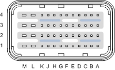
Table 2.1. Part numbers of the mating connector
| Supplier | Part number | Colour | Part |
|---|---|---|---|
| Molex | 64320-1318 | Grey | Female connector (left wire output) |
| 64320-1301 | Black | Wire cap |
Table 2.3. Part numbers for the 0.635 mm pin
| Supplier | Part number | Colour | Part |
|---|---|---|---|
| Molex | 64322-1039 | Tin | Female terminal, 1.40 mm - 1.70 mm wire insulation diameter |
| 64322-1029 | Female terminal, 1.60 mm - 1.90 mm wire insulation diameter | ||
| 64325-1010 | White | Plug for unused position | |
| Pins XA1, XA2, XA3, XA4, XB1, XB2, XB3, XB4, XB4+XC4, XC1, XC2, XC3, XC4, XD1, XD2, XD3, XD4, XE1, XE2, XE2+XF2, XE3, XE4, XE4+XF4, XF1, XF2, XF3, XF4, XG1, XG2, XG3, XG4, XH1, XH2+Z14, XH3+Z15, XH4, XJ1, XJ2+Z8, XJ3+Z9, XJ4, XJ4+XK4, XK1, XK2+Y8, XK3+Y9 and XK4 | |||
Table 2.4. Part numbers of the pin crimp tools
| Supplier | Part number | Part |
|---|---|---|
| Molex | 63811-9200 | Crimp tool for the 0.635 mm female terminal |
| 63811-8900 | Crimp tool for the 1.5 mm female terminal |
Table 2.5. Part numbers of the pin extraction tools
| Supplier | Part number | Part |
|---|---|---|
| Molex | 63813-2400 | Pin extraction tool for the 0.635 mm female terminal |
| 63813-2300 | Pin extraction tool for the 1.5 mm female terminal |
Table 2.6. Connector pinout — Bay X
| Main connector — Bay X | ||||||||
|---|---|---|---|---|---|---|---|---|
| Pin | P | Function | I/O | M | Loading | Filter | Range | Notes |
| XA1 | Spare | Not connected (reserved for daughterboard extensions). | ||||||
| SENT | I | 10k to VREFD | 86kHz | 0V to 5V | Available with the 'H-bridge and SENT' daughterboard. | |||
| XA2 | Spare | Not connected (reserved for daughterboard extensions). | ||||||
| SENT | I | 10k to VREFD | 86kHz | 0V to 5V | Available with the 'H-bridge and SENT' daughterboard. | |||
| XA3 | Spare | Not connected (reserved for daughterboard extensions). | ||||||
| SENT | I | 10k to VREFD | 86kHz | 0V to 5V | Available with the 'H-bridge and SENT' daughterboard. | |||
| XA4 | Spare | Not connected (reserved for daughterboard extensions). | ||||||
| SENT | I | 10k to VREFD | 86kHz | 0V to 5V | Available with the 'H-bridge and SENT' daughterboard. | |||
| XB1 | Digital | O | Y | Low side | 500mA | Typical use: cooling fan relay. Paired with VPWR for high-side. Related to internal channels DOT enable, Monitor (ct), Monitor (off ol), Monitor (requested state), Monitor (sb), Monitor (sg), Monitor (vcc uv) and Monitor (vdd uv). | ||
| XB2 | Analogue | I | 51k to VREFA | 44Hz | 0V to 5V | Typical use: variable geometry actuator position. 12-bit unsigned conversion, unscaled. | ||
| XB3 | Analogue | I | 51k to VREFB | 44Hz | 0V to 5V | Typical use: variable geometry actuator position. 12-bit unsigned conversion, unscaled. | ||
| XB4 | Spare | Y | Not connected (reserved for daughterboard extensions). Related to internal channels Monitor (c) and Monitor (v). | |||||
| Digital | O | H-bridge | 5A | Available with the 'H-bridge and SENT' daughterboard. Related to internal channels Monitor (c) and Monitor (v). | ||||
| XC1 | VGND | P | 1.5A | Rating specified at maximum operating temperature. XC1, XD3, XF1, XH1, Y2, Y4, Y26, Y27 and Z3 connected together internally. | ||||
| XC2 | Analogue | I | 51k to VGND | 44Hz | 0V to 5V | Typical use: throttle position sensor. 12-bit unsigned conversion, unscaled. Routed to the secondary processor for cross checking with the primary processor if required. Paired with XD2 for the purpose of cross checking the position of one throttle using two sensors. | ||
| XC3 | Analogue | I | 4k7 to VREFC | 11Hz | 0V to 5V | Typical use: oil temperature. Assigned to multiplexer A. Due to the multiplexer, which leaks current to the internal A/D channel, the input has a tolerance at mid range of +5.97% and -5.55%. 12-bit unsigned conversion, unscaled. | ||
| XC4 | Digital | O | Y | H-bridge | 5A | Available with the 'H-bridge and SENT' daughterboard. Related to internal channels Monitor (c) and Monitor (v). | ||
| Spare | Not connected (reserved for daughterboard extensions). Related to internal channels Monitor (c) and Monitor (v). | |||||||
| XD1 | Analogue (RTD) | I | 10k to VREFC | 114Hz | 0mV to 416.6mV | Typical use: exhaust manifold temperature. 12-bit unsigned conversion. To convert measured voltage (Vm) to actual voltage (Va) use the equation, Va=Vm/12. | ||
| XD2 | Analogue | I | 51k to VGND | 44Hz | 0V to 5V | Typical use: throttle position sensor. 12-bit unsigned conversion, unscaled. Routed to the secondary processor for cross checking with the primary processor if required. Paired with XC2 for the purpose of cross checking the position of one throttle using two sensors. | ||
| XD3 | VGND | P | 1.5A | Rating specified at maximum operating temperature. XC1, XD3, XF1, XH1, Y2, Y4, Y26, Y27 and Z3 connected together internally. | ||||
| XD4 | Constant current (inductive) | O | Y | Low side | 0A to 2A, 10.5Hz to 4000Hz | Typical use: wastegate valve. Paired with Y5 for high-side. Serial output. Related to internal channels DOT enable, DOT sync-phase, Monitor (enabled), Monitor (fault), Monitor (off ol), Monitor (on ol), Monitor (ov), Monitor (phase synced), Monitor (reset), Monitor (sb), Monitor (sb tested), Monitor (sg) and Monitor (sg+ol tested). | ||
| Digital | 2A, 10Hz to 4000Hz | |||||||
| XE1 | Analogue | I | 100k to VGND | 44Hz | 0V to 5V | Typical use: turbo outlet pressure. 12-bit unsigned conversion, unscaled. | ||
| XE2 | Spare | Y | Not connected (reserved for daughterboard extensions). Related to internal channels Monitor (c) and Monitor (v). | |||||
| Digital | O | H-bridge | 5A | Available with the 'H-bridge and SENT' daughterboard. Related to internal channels Monitor (c) and Monitor (v). | ||||
| XE3 | Digital | O | Low side | 500mA | Paired with VPWR for high-side. | |||
| XE4 | Spare | Y | Not connected (reserved for daughterboard extensions). Related to internal channels Monitor (c) and Monitor (v). | |||||
| Digital | O | H-bridge | 5A | Available with the 'H-bridge and SENT' daughterboard. Related to internal channels Monitor (c) and Monitor (v). | ||||
| XF1 | VGND | P | 1.5A | Rating specified at maximum operating temperature. XC1, XD3, XF1, XH1, Y2, Y4, Y26, Y27 and Z3 connected together internally. | ||||
| XF2 | Digital | O | Y | H-bridge | 5A | Available with the 'H-bridge and SENT' daughterboard. Related to internal channels Monitor (c) and Monitor (v). | ||
| Spare | Not connected (reserved for daughterboard extensions). Related to internal channels Monitor (c) and Monitor (v). | |||||||
| XF3 | Digital | I | 10k to VPWR | 33Hz | 0V to VPWR | Preferred voltage range is 0V to 5V. | ||
| SENT | 10k to VREFD | 86kHz | 0V to 5V | Available with ECU build option. | ||||
| Available with the 'H-bridge and SENT' daughterboard. | ||||||||
| XF4 | Digital | O | Y | H-bridge | 5A | Available with the 'H-bridge and SENT' daughterboard. Related to internal channels Monitor (c) and Monitor (v). | ||
| Spare | Not connected (reserved for daughterboard extensions). Related to internal channels Monitor (c) and Monitor (v). | |||||||
| XG1 | Analogue | I | 4k7 to VREFC | 11Hz | 0V to 5V | Typical use: ambient air temperature. 12-bit unsigned conversion, unscaled. | ||
| XG2 | Sensor supply | P | Y | 5V, 200mA | Sensor supply, VREFD. Can be turned on and off by the application for diagnostics purposes, see also: XG3. Related to internal channels DOT disable, Monitor (ct) and Monitor (v). | |||
| XG3 | Sensor ground | P | 2A | Sensor ground, VRTND, see also: XG2. | ||||
| XG4 | Digital | I | 10k to VREFD | 10kHz | 0V to 5V | Cam-shaft position sensor. | ||
| Secondary crank-shaft input position sensor. | ||||||||
| SENT | 86kHz | Available with ECU build option. | ||||||
| XH1 | VGND | P | 1.5A | Rating specified at maximum operating temperature. XC1, XD3, XF1, XH1, Y2, Y4, Y26, Y27 and Z3 connected together internally. | ||||
| XH2 | Sensor supply | P | Y | 5V, 200mA | Sensor supply, VREFC. Current capability listed is total for both VREFC supply pins. Can be turned on and off by the application for diagnostics purposes, see also: . Related to internal channels DOT disable, Monitor (ct) and Monitor (v). | |||
| XH3 | Sensor ground | P | 2A | Sensor ground, VRTNC. XH3 and Z15 connected together internally, see also: . | ||||
| XH4 | Digital | I | 10k to VREFD | 10kHz | 0V to 5V | Cam-shaft position sensor. | ||
| Secondary crank-shaft position sensor. | ||||||||
| SENT | 86kHz | Available with ECU build option. | ||||||
| XJ1 | Analogue (HEGO) | I | 453k to VREFB | 705Hz | 0V to 5V | The loading provides a small activation current for the HEGO sensor (approx. 10uA), for those sensors that require a current to maintain oxygen concentration in the reference chamber. 12-bit unsigned conversion, unscaled. | ||
| XJ2 | Sensor supply | P | Y | 5V, 200mA | Sensor supply, VREFB. Current capability listed is total for both VREFB supply pins. Can be turned on and off by the application for diagnostics purposes, see also: . Related to internal channels DOT disable, Monitor (ct) and Monitor (v). | |||
| XJ3 | Sensor ground | P | 2A | Sensor ground, VRTNB. XJ3 and Z9 connected together internally, see also: . | ||||
| XJ4 | Spare | Y | Not connected (reserved for daughterboard extensions). Related to internal channels Monitor (c) and Monitor (v). | |||||
| Digital | O | H-bridge | 5A | Available with the 'H-bridge and SENT' daughterboard. Related to internal channels Monitor (c) and Monitor (v). | ||||
| XK1 | Analogue (HEGO) | I | 453k to VREFA | 705Hz | 0V to 5V | The loading provides a small activation current for the HEGO sensor (approx. 10uA), for those sensors that require a current to maintain oxygen concentration in the reference chamber. 12-bit unsigned conversion, unscaled. | ||
| XK2 | Sensor supply | P | Y | 5V, 200mA | Sensor supply, VREFA. Current capability listed is total for both VREFA supply pins. Can be turned on and off by the application for diagnostics purposes, see also: . Related to internal channels DOT disable, Monitor (ct) and Monitor (v). | |||
| XK3 | Sensor ground | P | 2A | Sensor ground, VRTNA. XK3 and Y9 connected together internally, see also: . | ||||
| XK4 | Digital | O | Y | H-bridge | 5A | Available with the 'H-bridge and SENT' daughterboard. Related to internal channels Monitor (c) and Monitor (v). | ||
| Spare | Not connected (reserved for daughterboard extensions). Related to internal channels Monitor (c) and Monitor (v). | |||||||
| XL1 | Digital | O | Y | Low side | 4A | Typical use: HEGO heater. Paired with VPWR for high-side. Related to internal channels Monitor (ct) and Monitor (v). | ||
| XL2 | Constant current (inductive) | O | Y | Low side | 0A to 2A, 10.5Hz to 4000Hz | Paired with VPWR for high-side. Serial output. Related to internal channels DOT enable, DOT sync-phase, Monitor (enabled), Monitor (fault), Monitor (off ol), Monitor (on ol), Monitor (ov), Monitor (phase synced), Monitor (reset), Monitor (sb), Monitor (sb tested), Monitor (sg) and Monitor (sg+ol tested). | ||
| Digital | 2A, 10Hz to 4000Hz | |||||||
| XL3 | Digital | O | Y | Low side | 1A | Paired with VPWR for high-side. Related to internal channels DOT enable, Monitor (ct), Monitor (off ol), Monitor (requested state), Monitor (sb), Monitor (sg), Monitor (vcc uv) and Monitor (vdd uv). | ||
| XL4 | Digital | O | Y | Half bridge, low or high side | 8A | Related to internal channels DOT select-hs, Monitor (c), Monitor (ct) and Monitor (v). | ||
| H-bridge | 10A | Typical use: electronic throttle (XL4 + XM4). Related to internal channels DOT select-hs, Monitor (c), Monitor (ct) and Monitor (v). | ||||||
| XM1 | Digital | O | Y | Low side | 4A | Typical use: HEGO heater. Paired with VPWR for high-side. Related to internal channels Monitor (ct) and Monitor (v). | ||
| XM2 | Digital | O | Y | H-bridge | 5A | Typical use: variable geometry turbocharger. Related to internal channels Monitor (ct), Monitor (no fault) and Monitor (v). | ||
| XM3 | Digital | O | Y | H-bridge | 5A | Typical use: variable geometry turbocharger. Related to internal channels Monitor (ct), Monitor (no fault) and Monitor (v). | ||
| XM4 | Digital | O | Y | H-bridge | 10A | Typical use: electronic throttle (XL4 + XM4). Related to internal channels DOT select-hs, Monitor (c), Monitor (ct) and Monitor (v). | ||
| Half bridge, low or high side | 8A | Related to internal channels DOT select-hs, Monitor (c), Monitor (ct) and Monitor (v). | ||||||
Connector packs can be ordered from Pi. Individual connector components can be ordered from Pi or from various manufacturers.
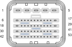
Table 2.7. Part numbers of the mating connector
| Supplier | Part number | Colour | Part |
|---|---|---|---|
| Molex | 64321-2019 | Brown | Female connector (right wire output) |
| 64321-1101 | Black | Wire cap |
Table 2.8. Part numbers for the 2.8 mm pin
| Supplier | Part number | Colour | Part |
|---|---|---|---|
| Molex | 64324-1029 | Tin | Female terminal, 1.60 mm - 1.90 mm wire insulation diameter |
| 64324-1019 | Female terminal, 3.40 mm - 4.00 mm wire insulation diameter | ||
| 64325-1358 | Grey | Single wire seal, 2.65 mm - 3.45 mm wire insulation diameter | |
| 64325-1366 | Single wire seal, 3.50 mm - 4.21 mm wire insulation diameter | ||
| 64325-1091 | Black | Plug for unused position | |
| Pins Y1, Y2, Y3, Y4 and Y5 | |||
Table 2.10. Part numbers for the 0.635 mm pin
| Supplier | Part number | Colour | Part |
|---|---|---|---|
| Molex | 64322-1039 | Tin | Female terminal, 1.40 mm - 1.70 mm wire insulation diameter |
| 64322-1029 | Female terminal, 1.60 mm - 1.90 mm wire insulation diameter | ||
| 64325-1010 | White | Plug for unused position | |
| Pins Y7, Y10, Y11, Y12, Y13, Y14, Y15, Y16, Y19, Y20, Y21, Y22, Y23, Y24, Y25, Y26, Y27, Y28, Y31, Y32, Y33, Y34, Y35, Y36, Y37, Y38, Y39, Y40, Y43, Y44, Y45, Y46, Y47, Y48, Y49, Y50 and Y51+Y52 | |||
Table 2.11. Part numbers of the pin crimp tools
| Supplier | Part number | Part |
|---|---|---|
| Molex | 63811-9200 | Crimp tool for the 0.635 mm female terminal |
| 63811-8900 | Crimp tool for the 1.5 mm female terminal | |
| 63811-9800 | Crimp tool for the 2.8 mm female terminal |
Table 2.12. Part numbers of the pin extraction tools
| Supplier | Part number | Part |
|---|---|---|
| Molex | 63813-2400 | Pin extraction tool for the 0.635 mm female terminal |
| 63813-2300 | Pin extraction tool for the 1.5 mm female terminal | |
| 63813-2500 | Pin extraction tool for the 2.8 mm female terminal |
Table 2.13. Connector pinout — Bay Y
| Main connector — Bay Y | ||||||||
|---|---|---|---|---|---|---|---|---|
| Pin | P | Function | I/O | M | Loading | Filter | Range | Notes |
| Y1 | Actuator supply | P | Y | High side | 10A | Non-injector high-side actuator power. To achieve the current carrying capability of this pin, the maximum wire gauge allowed in the wire harness must be used. Related to internal channels DOT reset, DOT, Monitor (c), Monitor (ct), Monitor (d), Monitor (fail-safe disabled), Monitor (no fault), Monitor (off ol), Monitor (on ol), Monitor (ot warning), Monitor (ov), Monitor (power-on reset), Monitor (requested state), Monitor (sb), Monitor (severe short circuit) and Monitor (uv). | ||
| Y2 | VGND | P | 13.5A | Rating specified at maximum operating temperature. To achieve the current carrying capability of this pin, the maximum wire gauge allowed in the wire harness must be used. XC1, XD3, XF1, XH1, Y2, Y4, Y26, Y27 and Z3 connected together internally. | ||||
| Y3 | VPWR | P | Y | 13.5A | Rating specified at maximum operating temperature. To achieve the current carrying capability of this pin, the maximum wire gauge allowed in the wire harness must be used, see also: Z2 and Z4. Related to internal channel AIN VPWR. | |||
| Y4 | VGND | P | 13.5A | Rating specified at maximum operating temperature. To achieve the current carrying capability of this pin, the maximum wire gauge allowed in the wire harness must be used. XC1, XD3, XF1, XH1, Y2, Y4, Y26, Y27 and Z3 connected together internally. | ||||
| Y5 | Actuator supply | P | Y | High side | 10A | Non-injector high-side actuator power. To achieve the current carrying capability of this pin, the maximum wire gauge allowed in the wire harness must be used. Related to internal channels DOT reset, DOT, Monitor (c), Monitor (ct), Monitor (d), Monitor (fail-safe disabled), Monitor (no fault), Monitor (off ol), Monitor (on ol), Monitor (ot warning), Monitor (ov), Monitor (power-on reset), Monitor (requested state), Monitor (sb), Monitor (severe short circuit) and Monitor (uv). | ||
| Y6 | Digital | O | Y | Low side | 8A | Typical use: lift pump control. Paired with VPWR for high-side. Related to internal channels Monitor (ct) and Monitor (v). | ||
| Y7 | Constant current (inductive) | O | Y | Low side | 0A to 2A, 10.5Hz to 4000Hz | Typical use: intake variable value actuation. Paired with Y1 for high-side. Serial output. Related to internal channels DOT enable, DOT sync-phase, Monitor (enabled), Monitor (fault), Monitor (off ol), Monitor (on ol), Monitor (ov), Monitor (phase synced), Monitor (reset), Monitor (sb), Monitor (sb tested), Monitor (sg) and Monitor (sg+ol tested). | ||
| Digital | 2A, 10Hz to 4000Hz | |||||||
| Y8 | Sensor supply | P | Y | 5V, 200mA | Sensor supply, VREFA. Current capability listed is total for both VREFA supply pins. Can be turned on and off by the application for diagnostics purposes, see also: . Related to internal channels DOT disable, Monitor (ct) and Monitor (v). | |||
| Y9 | Sensor ground | P | 2A | Sensor ground, VRTNA. XK3 and Y9 connected together internally, see also: . | ||||
| Y10 | Constant current (inductive) | O | Y | Low side | 0A to 2A, 10.5Hz to 4000Hz | Typical use: intake variable value actuation. Paired with Y5 for high-side. Serial output. Related to internal channels DOT enable, DOT sync-phase, Monitor (enabled), Monitor (fault), Monitor (off ol), Monitor (on ol), Monitor (ov), Monitor (phase synced), Monitor (reset), Monitor (sb), Monitor (sb tested), Monitor (sg) and Monitor (sg+ol tested). | ||
| Digital | 2A, 10Hz to 4000Hz | |||||||
| Y11 | CAN- (low) | C | 120R | CAN bus A low (-ve). Default CAN bus for reprogramming unless overridden by the application, see also: Y12. Related to internal channels DOT disable-CAN and Monitor (CAN A+B no fault). | ||||
| Y12 | CAN+ (high) | C | 120R | CAN bus A high (+ve). Default CAN bus for reprogramming unless overridden by the application, see also: Y11. Related to internal channels DOT disable-CAN and Monitor (CAN A+B no fault). | ||||
| Y13 | Constant current (inductive) | O | Y | Low side | 0A to 2A, 10.5Hz to 4000Hz | Typical use: exhaust variable value actuation. Paired with Y1 for high-side. Serial output. Related to internal channels DOT enable, DOT sync-phase, Monitor (enabled), Monitor (fault), Monitor (off ol), Monitor (on ol), Monitor (ov), Monitor (phase synced), Monitor (reset), Monitor (sb), Monitor (sb tested), Monitor (sg) and Monitor (sg+ol tested). | ||
| Digital | 2A, 10Hz to 4000Hz | |||||||
| Y14 | Digital | I | 10k to VREFD | 10kHz | 0V to 5V | Cam-shaft position sensor. | ||
| Secondary crank-shaft position sensor. | ||||||||
| Y15 | Digital | I | 10k to VREFD | 10kHz | 0V to 5V | Cam-shaft position sensor. | ||
| Secondary crank-shaft position sensor. | ||||||||
| Y16 | Constant current (inductive) | O | Y | Low side | 0A to 2A, 10.5Hz to 4000Hz | Typical use: exhaust variable value actuation. Paired with Y5 for high-side. Serial output. Related to internal channels DOT enable, DOT sync-phase, Monitor (enabled), Monitor (fault), Monitor (off ol), Monitor (on ol), Monitor (ov), Monitor (phase synced), Monitor (reset), Monitor (sb), Monitor (sb tested), Monitor (sg) and Monitor (sg+ol tested). | ||
| Digital | 2A, 10Hz to 4000Hz | |||||||
| Y17 | Constant current (inductive) | O | Y | Low side | 0A to 2A, 10.5Hz to 4000Hz | Typical use: wastegate valve. Paired with Y1 for high-side. Serial output. Related to internal channels DOT enable, DOT sync-phase, Monitor (enabled), Monitor (fault), Monitor (off ol), Monitor (on ol), Monitor (ov), Monitor (phase synced), Monitor (reset), Monitor (sb), Monitor (sb tested), Monitor (sg) and Monitor (sg+ol tested). | ||
| Digital | 2A, 10Hz to 4000Hz | |||||||
| Y18 | Digital | O | Y | Low side | 6A/4A | Typical use: fuel control valve. Paired with Y1 for high-side. Related to internal channels DOT enable, DOT reset clock bank A, DOT reset-fault bank A, Monitor (checksum fault bank A), Monitor (clock fault bank A), Monitor (ct), Monitor (enabled), Monitor (hs sb), Monitor (hs sg), Monitor (ls ol), Monitor (ls sb), Monitor (ls sg), Monitor (ot bank A), Monitor (self-test pass bank A), Monitor (self-test run bank A), Monitor (uvcc5 bank A), Monitor (uvccp bank A) and Monitor (v). | ||
| Y19 | Analogue | I | 4k7 to VREFC | 11Hz | 0V to 5V | Typical use: fuel rail temperature. 12-bit unsigned conversion, unscaled. | ||
| Y20 | Digital | I | 5k1 to VREFD | 106kHz | 0V to 5V | Typical use: turbo speed, or other high-speed frequency input. | ||
| Y21 | Digital | I | 5k1 to VREFD | 106kHz | 0V to 5V | Typical use: turbo speed, or other high-speed frequency input. | ||
| Y22 | FEPS | I | 87k2 to 2.62V | 323Hz | ±18V | Module flash programming control. | ||
| Y23 | CAN- (low) | C | No termination resistor | CAN bus B low (-ve), see also: Y24. Related to internal channels DOT disable-CAN and Monitor (CAN A+B no fault). | ||||
| Y24 | CAN+ (high) | C | No termination resistor | CAN bus B high (+ve), see also: Y23. Related to internal channels DOT disable-CAN and Monitor (CAN A+B no fault). | ||||
| Y25 | Digital | I | 10k to VGND | 33Hz | 0V to VPWR | Key position (ignition sense) input. Routed to the secondary processor for cross checking with the primary processor if required. A voltage higher than 2.9V worst case will wake up the ECU. Related to internal channel DOT enable-PSU-hold. | ||
| Y26 | VGND | P | 1.5A | Rating specified at maximum operating temperature. XC1, XD3, XF1, XH1, Y2, Y4, Y26, Y27 and Z3 connected together internally. | ||||
| Y27 | VGND | P | 1.5A | Rating specified at maximum operating temperature. XC1, XD3, XF1, XH1, Y2, Y4, Y26, Y27 and Z3 connected together internally. | ||||
| Y28 | Flash code | O | Y | Low side | 500mA | ECU status information. Paired with VPWR for high-side. Related to internal channels DOT enable, Monitor (ct), Monitor (off ol), Monitor (requested state), Monitor (sb), Monitor (sg), Monitor (vcc uv) and Monitor (vdd uv). | ||
| Y29 | Digital | O | Y | Low side | 4A | Heater for UEGO A. Paired with Y1 or VPWR for high-side. This pin can be used as a generic low-side driver. When using the UEGO A sensor, this pin can be used for the heater pin as it provides internal diagnostic feedback to the sensor. A higher current pin can be used to drive the UEGO A sensor heater when using the sensor in below ambient temperatures or when using a 24 volt system. See the 'Oxygen sensing - wide band UEGO' section for further details, see also: Z10, Z11, Z22 and Z23. Related to internal channels Monitor (ct), Monitor (ol), Monitor (sb), Monitor (sg) and Monitor (v). | ||
| Y30 | Digital | O | Y | Half bridge, low or high side | 8A | Related to internal channels DOT select-hs, Monitor (c), Monitor (ct) and Monitor (v). | ||
| H-bridge | 10A | Typical use: electronic throttle (Y30 + Y42). Related to internal channels DOT select-hs, Monitor (c), Monitor (ct) and Monitor (v). | ||||||
| Y31 | Analogue | I | 100k to VREFA | 1129Hz | 0V to 5V | Typical use: manifold air flow. 12-bit unsigned conversion, unscaled. | ||
| Y32 | Analogue (VRS diff., +ve) | I | 10k to VREFB | 23kHz | ±220V | Primary crank-shaft position sensor, see also: Y33. Related to internal channels DOT select Hall-effect bias and DOT select Hall-effect. | ||
| Analogue (VRS single ended) | ±110V | |||||||
| Digital (Hall) | 0V to 5V | Primary crank-shaft position sensor. Related to internal channels DOT select Hall-effect bias and DOT select Hall-effect. | ||||||
| Y33 | Analogue (VRS diff., -ve) | I | ±220V | Crank-shaft position sensor. Connect to ground while operating with a Hall effect sensor or with a single ended VRS on Y32. Related to internal channels DOT select Hall-effect bias and DOT select Hall-effect. | ||||
| Y34 | Digital | I | 10k to VPWR | 33Hz | 0V to VPWR | Typical use: dash switch. Preferred voltage range is 0V to 5V. | ||
| Y35 | CAN- (low) | C | No termination resistor | CAN bus C low (-ve), see also: Y36. Related to internal channel DOT disable-CAN. | ||||
| Y36 | CAN+ (high) | C | No termination resistor | CAN bus C high (+ve), see also: Y35. Related to internal channel DOT disable-CAN. | ||||
| Y37 | Digital | O | Y | 5k1 to VREFD | 1A | Typical use: smart spark actuation. Paired with VPWR for high-side. Related to internal channels Monitor (ct) and Monitor (d). | ||
| Low side | Coil/spark (smart) driver. Related to internal channels Monitor (ct) and Monitor (d). | |||||||
| Y38 | Digital | O | Y | 5k1 to VREFD | 1A | Typical use: smart spark actuation. Paired with VPWR for high-side. Related to internal channels Monitor (ct) and Monitor (d). | ||
| Low side | Coil/spark (smart) driver. Related to internal channels Monitor (ct) and Monitor (d). | |||||||
| Y39 | Digital | O | Y | 5k1 to VREFD | 1A | Typical use: smart spark actuation. Paired with VPWR for high-side. Related to internal channels Monitor (ct) and Monitor (d). | ||
| Low side | Coil/spark (smart) driver. Related to internal channels Monitor (ct) and Monitor (d). | |||||||
| Y40 | Digital | O | Y | 5k1 to VREFD | 1A | Typical use: smart spark actuation. Paired with VPWR for high-side. Related to internal channels Monitor (ct) and Monitor (d). | ||
| Low side | Coil/spark (smart) driver. Related to internal channels Monitor (ct) and Monitor (d). | |||||||
| Y41 | Digital | O | Y | Low side | 4A | Heater for UEGO B. Paired with Y5 or VPWR for high-side. This pin can be used as a generic low-side driver. When using the UEGO B sensor, this pin can be used for the heater pin as it provides internal diagnostic feedback to the sensor. A higher current pin can be used to drive the UEGO B sensor heater when using the sensor in below ambient temperatures or when using a 24 volt system. See the 'Oxygen sensing - wide band UEGO' section for further details, see also: Z34, Z35, Z46 and Z47. Related to internal channels Monitor (ct), Monitor (ol), Monitor (sb), Monitor (sg) and Monitor (v). | ||
| Y42 | Digital | O | Y | H-bridge | 10A | Typical use: electronic throttle (Y30 + Y42). Related to internal channels DOT select-hs, Monitor (c), Monitor (ct) and Monitor (v). | ||
| Half bridge, low or high side | 8A | Related to internal channels DOT select-hs, Monitor (c), Monitor (ct) and Monitor (v). | ||||||
| Y43 | Digital | I | 5k1 to VREFD | 10kHz | 0V to 5V | Typical use: vehicle speed. | ||
| Y44 | Digital | O | Y | 5k1 to VREFD | 1A | Typical use: smart spark actuation. Paired with VPWR for high-side. Related to internal channels Monitor (ct) and Monitor (d). | ||
| Low side | Coil/spark (smart) driver. Related to internal channels Monitor (ct) and Monitor (d). | |||||||
| Y45 | Digital | O | Y | 5k1 to VREFD | 1A | Typical use: smart spark actuation. Paired with VPWR for high-side. Related to internal channels Monitor (ct) and Monitor (d). | ||
| Low side | Coil/spark (smart) driver. Related to internal channels Monitor (ct) and Monitor (d). | |||||||
| Y46 | Digital | I | 10k to VGND | 33Hz | 0V to 5V | Typical use: dash switch. | ||
| Y47 | CAN- (low) | C | No termination resistor | CAN bus D low (-ve), see also: Y48. Related to internal channel DOT disable-CAN. | ||||
| Y48 | CAN+ (high) | C | No termination resistor | CAN bus D high (+ve), see also: Y47. Related to internal channel DOT disable-CAN. | ||||
| Y49 | Digital | O | Y | 5k1 to VREFD | 1A | Typical use: smart spark actuation. Paired with VPWR for high-side. Related to internal channels Monitor (ct) and Monitor (d). | ||
| Low side | Coil/spark (smart) driver. Related to internal channels Monitor (ct) and Monitor (d). | |||||||
| Y50 | Digital | O | Y | 5k1 to VREFD | 1A | Typical use: smart spark actuation. Paired with VPWR for high-side. Related to internal channels Monitor (ct) and Monitor (d). | ||
| Low side | Coil/spark (smart) driver. Related to internal channels Monitor (ct) and Monitor (d). | |||||||
| Y51 | Knock Sensor | I | 1M to VGND | 20kHz | 0V to 10V | Knock sensor B. Related to internal channels AIN, AIN and KNOCK. | ||
| Y52 | Knock Sensor | I | 1M to VGND | 20kHz | 0V to 10V | Knock sensor B. Related to internal channels AIN, AIN and KNOCK. | ||
| Y53 | Digital | O | Y | Low side | 6A/4A | Typical use: pressure regulation valve. Paired with Y5 for high-side. Related to internal channels DOT enable, DOT reset clock bank B, DOT reset-fault bank B, Monitor (checksum fault bank B), Monitor (clock fault bank B), Monitor (ct), Monitor (enabled), Monitor (hs sb), Monitor (hs sg), Monitor (ls ol), Monitor (ls sb), Monitor (ls sg), Monitor (ot bank B), Monitor (self-test pass bank B), Monitor (self-test run bank B), Monitor (uvcc5 bank B), Monitor (uvccp bank B) and Monitor (v). | ||
Connector packs can be ordered from Pi. Individual connector components can be ordered from Pi or from various manufacturers.
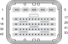
Table 2.14. Part numbers of the mating connector
| Supplier | Part number | Colour | Part |
|---|---|---|---|
| Molex | 64321-2011 | Black | Female connector (right wire output) |
| 64321-1101 | Wire cap |
Table 2.15. Part numbers for the 2.8 mm pin
| Supplier | Part number | Colour | Part |
|---|---|---|---|
| Molex | 64324-1029 | Tin | Female terminal, 1.60 mm - 1.90 mm wire insulation diameter |
| 64324-1019 | Female terminal, 3.40 mm - 4.00 mm wire insulation diameter | ||
| 64325-1358 | Grey | Single wire seal, 2.65 mm - 3.45 mm wire insulation diameter | |
| 64325-1366 | Single wire seal, 3.50 mm - 4.21 mm wire insulation diameter | ||
| 64325-1091 | Black | Plug for unused position | |
| Pins Z1, Z2, Z3, Z4 and Z5 | |||
Table 2.17. Part numbers for the 0.635 mm pin
| Supplier | Part number | Colour | Part |
|---|---|---|---|
| Molex | 64322-1039 | Tin | Female terminal, 1.40 mm - 1.70 mm wire insulation diameter |
| 64322-1029 | Female terminal, 1.60 mm - 1.90 mm wire insulation diameter | ||
| 64325-1010 | White | Plug for unused position | |
| Pins Z7, Z10, Z11, Z12, Z13, Z16, Z19, Z20, Z21, Z22, Z23, Z24, Z25, Z26, Z27, Z28, Z31, Z32, Z33, Z34, Z35, Z36, Z37, Z38, Z39, Z40, Z43, Z44, Z45, Z46, Z47, Z48+Z49, Z50, Z51 and Z52 | |||
Table 2.18. Part numbers of the pin crimp tools
| Supplier | Part number | Part |
|---|---|---|
| Molex | 63811-9200 | Crimp tool for the 0.635 mm female terminal |
| 63811-8900 | Crimp tool for the 1.5 mm female terminal | |
| 63811-9800 | Crimp tool for the 2.8 mm female terminal |
Table 2.19. Part numbers of the pin extraction tools
| Supplier | Part number | Part |
|---|---|---|
| Molex | 63813-2400 | Pin extraction tool for the 0.635 mm female terminal |
| 63813-2300 | Pin extraction tool for the 1.5 mm female terminal | |
| 63813-2500 | Pin extraction tool for the 2.8 mm female terminal |
Table 2.20. Connector pinout — Bay Z
| Main connector — Bay Z | ||||||||
|---|---|---|---|---|---|---|---|---|
| Pin | P | Function | I/O | M | Loading | Filter | Range | Notes |
| Z1 | Actuator supply injector bank A | P | Y | High side | 13A RMS, 25A peak | Injector high-side boost/battery supply, bank A. To achieve the current carrying capability of this pin, the maximum wire gauge allowed in the wire harness must be used. Maximum boost setpoint is 65V, see also: Z6, Z18, Z30 and Z42. Related to internal channels DOT enable, DOT reset clock bank A, DOT reset-fault bank A, Monitor (checksum fault bank A), Monitor (clock fault bank A), Monitor (ct), Monitor (enabled), Monitor (max recharge time), Monitor (ot bank A), Monitor (ov), Monitor (recharge time), Monitor (self-test pass bank A), Monitor (self-test run bank A), Monitor (uvcc5 bank A), Monitor (uvccp bank A) and Monitor (v). | ||
| Z2 | VPWR | P | Y | 13.5A | Rating specified at maximum operating temperature. To achieve the current carrying capability of this pin, the maximum wire gauge allowed in the wire harness must be used, see also: Y3 and Z4. Related to internal channel AIN VPWR. | |||
| Z3 | VGND | P | 13.5A | Rating specified at maximum operating temperature. To achieve the current carrying capability of this pin, the maximum wire gauge allowed in the wire harness must be used. XC1, XD3, XF1, XH1, Y2, Y4, Y26, Y27 and Z3 connected together internally. | ||||
| Z4 | VPWR | P | Y | 13.5A | Rating specified at maximum operating temperature. To achieve the current carrying capability of this pin, the maximum wire gauge allowed in the wire harness must be used, see also: Y3 and Z2. Related to internal channel AIN VPWR. | |||
| Z5 | Actuator supply injector bank B | P | Y | High side | 13A RMS, 25A peak | Injector high-side boost/battery supply. To achieve the current carrying capability of this pin, the maximum wire gauge allowed in the wire harness must be used. Maximum boost setpoint is 65V, see also: Z17, Z29, Z41 and Z53. Related to internal channels DOT enable, DOT reset clock bank B, DOT reset-fault bank B, Monitor (checksum fault bank B), Monitor (clock fault bank B), Monitor (ct), Monitor (enabled), Monitor (max recharge time), Monitor (ot bank B), Monitor (ov), Monitor (recharge time), Monitor (self-test pass bank B), Monitor (self-test run bank B), Monitor (uvcc5 bank B), Monitor (uvccp bank B) and Monitor (v). | ||
| Z6 | Digital (injector) | O | Y | Low side | 15A | Fuel injector A1. Paired with Z1 for high-side. Not populated on M670N, use Y18 instead. Related to internal channels DOT enable, DOT reset clock bank A, DOT reset-fault bank A, Monitor (boost oc), Monitor (checksum fault bank A), Monitor (clock fault bank A), Monitor (ct), Monitor (enabled), Monitor (hs sb), Monitor (hs sg), Monitor (ls ol), Monitor (ls sb), Monitor (ls sg), Monitor (ot bank A), Monitor (self-test pass bank A), Monitor (self-test run bank A), Monitor (uvcc5 bank A) and Monitor (uvccp bank A). | ||
| Z7 | Constant current (inductive) | O | Y | Low side | 0A to 2A, 10.5Hz to 4000Hz | Typical use: exhaust gas recirculation actuation. Paired with VPWR for high-side. Serial output. Related to internal channels DOT enable, DOT sync-phase, Monitor (enabled), Monitor (fault), Monitor (off ol), Monitor (on ol), Monitor (ov), Monitor (phase synced), Monitor (reset), Monitor (sb), Monitor (sb tested), Monitor (sg) and Monitor (sg+ol tested). | ||
| Digital | 2A, 10Hz to 4000Hz | |||||||
| Z8 | Sensor supply | P | Y | 5V, 200mA | Sensor supply, VREFB. Current capability listed is total for both VREFB supply pins. Can be turned on and off by the application for diagnostics purposes, see also: . Related to internal channels DOT disable, Monitor (ct) and Monitor (v). | |||
| Z9 | Sensor ground | P | 2A | Sensor ground, VRTNB. XJ3 and Z9 connected together internally, see also: . | ||||
| Z10 | UEGO sensor A RE+ (aka UN) | Y | n/a | n/a | n/a | Nernst Voltage for UEGO A (inverting input of pump current control respective in-/output for Ri-measurement), see also: Y29, Z11, Z22 and Z23. Related to internal channels AIN UA UEGO-A, AIN UR UEGO-A, Monitor (sb) and Monitor (sg). | ||
| Z11 | UEGO sensor A IPN (aka VM). | Y | n/a | n/a | n/a | Virtual ground for UEGO A (virtual ground of pump current control and of the LSU (0.5 VCC)), see also: Y29, Z10, Z22 and Z23. Related to internal channels AIN UA UEGO-A, AIN UR UEGO-A, Monitor (sb) and Monitor (sg). | ||
| Z12 | Digital | I | 10k to VPWR | 33Hz | 0V to VPWR | Typical use: low oil switch. Routed to the secondary processor for cross checking with the primary processor if required. Preferred voltage range is 0V to 5V. | ||
| Z13 | Digital | I | 10k to VGND | 33Hz | 0V to 5V | Typical use: brake switch. Routed to the secondary processor for cross checking with the primary processor if required. | ||
| Z14 | Sensor supply | P | Y | 5V, 200mA | Sensor supply, VREFC. Current capability listed is total for both VREFC supply pins. Can be turned on and off by the application for diagnostics purposes, see also: . Related to internal channels DOT disable, Monitor (ct) and Monitor (v). | |||
| Z15 | Sensor ground | P | 2A | Sensor ground, VRTNC. XH3 and Z15 connected together internally, see also: . | ||||
| Z16 | Analogue | I | 100k to VGND | 44Hz | 0V to 5V | Typical use: oil pressure. 12-bit unsigned conversion, unscaled. | ||
| Z17 | Digital (injector) | O | Y | Low side | 15A | Fuel injector B1. Paired with Z5 for high-side. Not populated on M670N, use Y53 instead. Related to internal channels DOT enable, DOT reset clock bank B, DOT reset-fault bank B, Monitor (boost oc), Monitor (checksum fault bank B), Monitor (clock fault bank B), Monitor (ct), Monitor (enabled), Monitor (hs sb), Monitor (hs sg), Monitor (ls ol), Monitor (ls sb), Monitor (ls sg), Monitor (ot bank B), Monitor (self-test pass bank B), Monitor (self-test run bank B), Monitor (uvcc5 bank B) and Monitor (uvccp bank B). | ||
| Z18 | Digital (injector) | O | Y | Low side | 15A | Fuel injector A2. Paired with Z1 for high-side. Related to internal channels DOT enable, DOT reset clock bank A, DOT reset-fault bank A, Monitor (boost oc), Monitor (checksum fault bank A), Monitor (clock fault bank A), Monitor (ct), Monitor (enabled), Monitor (hs sb), Monitor (hs sg), Monitor (ls ol), Monitor (ls sb), Monitor (ls sg), Monitor (ot bank A), Monitor (self-test pass bank A), Monitor (self-test run bank A), Monitor (uvcc5 bank A) and Monitor (uvccp bank A). | ||
| Z19 | Digital | O | Low side | 500mA | Power hold relay. Turned on when ECU is woken up, turned off when the ECU shuts down. No software control. | |||
| Z20 | Analogue | I | 51k to VREFB | 44Hz | 0V to 5V | Typical use: throttle position sensor. 12-bit unsigned conversion, unscaled. Routed to the secondary processor for cross checking with the primary processor if required. Paired with Z21 for the purpose of cross checking the position of one throttle using two sensors. | ||
| Z21 | Analogue | I | 51k to VREFA | 44Hz | 0V to 5V | Typical use: throttle position sensor. 12-bit unsigned conversion, unscaled. Routed to the secondary processor for cross checking with the primary processor if required. Paired with Z20 for the purpose of cross checking the position of one throttle using two sensors. | ||
| Z22 | UEGO sensor A RT (aka IA) | Y | n/a | n/a | n/a | Trim current for UEGO A (non-inverting input of pump current amplifier and output of the pump current control). Many sensors do not have this pin and thus this can be left disconnected, see also: Y29, Z10, Z11 and Z23. Related to internal channels AIN UA UEGO-A, AIN UR UEGO-A, Monitor (sb) and Monitor (sg). | ||
| Z23 | UEGO sensor A APE (aka IP). | Y | n/a | n/a | n/a | Pumping current for UEGO A (inverting input of pump current amplifier (shunt voltage)), see also: Y29, Z10, Z11 and Z22. Related to internal channels AIN UA UEGO-A, AIN UR UEGO-A, Monitor (sb) and Monitor (sg). | ||
| Z24 | Analogue | I | 100k to VREFA | 44Hz | 0V to 5V | Typical use: exhaust manifold pressure. 12-bit unsigned conversion, unscaled. | ||
| Z25 | Analogue | I | 100k to VREFB | 44Hz | 0V to 5V | Typical use: exhaust manifold pressure. 12-bit unsigned conversion, unscaled. | ||
| Z26 | Analogue (RTD) | I | 10k to VREFC | 114Hz | 0mV to 416.6mV | Typical use: exhaust manifold temperature. 12-bit unsigned conversion. To convert measured voltage (Vm) to actual voltage (Va) use the equation, Va=Vm/12. | ||
| Z27 | Analogue | I | 51k to VGND | 44Hz | 0V to 5V | Typical use: pedal position. 12-bit unsigned conversion, unscaled. Routed to the secondary processor for cross checking with the primary processor if required. Paired with Z28 for the purpose of cross checking the position of one pedal using two sensors. | ||
| Z28 | Analogue | I | 51k to VGND | 44Hz | 0V to 5V | Typical use: pedal position. 12-bit unsigned conversion, unscaled. Routed to the secondary processor for cross checking with the primary processor if required. Paired with Z27 for the purpose of cross checking the position of one pedal using two sensors. | ||
| Z29 | Digital (injector) | O | Y | Low side | 15A | Fuel injector B2. Paired with Z5 for high-side. Related to internal channels DOT enable, DOT reset clock bank B, DOT reset-fault bank B, Monitor (boost oc), Monitor (checksum fault bank B), Monitor (clock fault bank B), Monitor (ct), Monitor (enabled), Monitor (hs sb), Monitor (hs sg), Monitor (ls ol), Monitor (ls sb), Monitor (ls sg), Monitor (ot bank B), Monitor (self-test pass bank B), Monitor (self-test run bank B), Monitor (uvcc5 bank B) and Monitor (uvccp bank B). | ||
| Z30 | Digital (injector) | O | Y | Low side | 15A | Fuel injector A3. Paired with Z1 for high-side. Related to internal channels DOT enable, DOT reset clock bank A, DOT reset-fault bank A, Monitor (boost oc), Monitor (checksum fault bank A), Monitor (clock fault bank A), Monitor (ct), Monitor (enabled), Monitor (hs sb), Monitor (hs sg), Monitor (ls ol), Monitor (ls sb), Monitor (ls sg), Monitor (ot bank A), Monitor (self-test pass bank A), Monitor (self-test run bank A), Monitor (uvcc5 bank A) and Monitor (uvccp bank A). | ||
| Z31 | Digital | O | Y | Low side | 500mA | Typical use: glow plug relay or cylinder deactivation relay. Paired with VPWR for high-side. Related to internal channels DOT enable, Monitor (ct), Monitor (off ol), Monitor (requested state), Monitor (sb), Monitor (sg), Monitor (vcc uv) and Monitor (vdd uv). | ||
| Z32 | Analogue | I | 100k to VGND | 44Hz | 0V to 5V | Typical use: turbo outlet pressure. 12-bit unsigned conversion, unscaled. | ||
| Z33 | Analogue | I | 100k to VGND | 44Hz | 0V to 5V | Typical use: barometric pressure. 12-bit unsigned conversion, unscaled. | ||
| Z34 | UEGO sensor B RE+ (aka UN). | Y | n/a | n/a | n/a | Nernst Voltage for UEGO B (inverting input of pump current control respective in-/output for Ri-measurement), see also: Y41, Z35, Z46 and Z47. Related to internal channels AIN UA UEGO-B, AIN UR UEGO-B, Monitor (sb) and Monitor (sg). | ||
| Z35 | UEGO sensor B IPN (aka VM) | Y | n/a | n/a | n/a | Virtual ground for UEGO B (virtual ground of pump current control and of the LSU (0.5 VCC)), see also: Y41, Z34, Z46 and Z47. Related to internal channels AIN UA UEGO-B, AIN UR UEGO-B, Monitor (sb) and Monitor (sg). | ||
| Z36 | Digital | O | Y | Low side | 500mA | Typical use: low oil level lamp. Paired with VPWR for high-side. Related to internal channels DOT enable, Monitor (ct), Monitor (off ol), Monitor (requested state), Monitor (sb), Monitor (sg), Monitor (vcc uv) and Monitor (vdd uv). | ||
| Z37 | Digital | O | Y | Low side | 500mA | Typical use: low oil pressure lamp. Paired with VPWR for high-side. Related to internal channels DOT enable, Monitor (ct), Monitor (off ol), Monitor (requested state), Monitor (sb), Monitor (sg), Monitor (vcc uv) and Monitor (vdd uv). | ||
| Z38 | Digital | O | Y | Low side | 500mA | Typical use: coolant temperature warning lamp. Paired with VPWR for high-side. Related to internal channels DOT enable, Monitor (ct), Monitor (off ol), Monitor (requested state), Monitor (sb), Monitor (sg), Monitor (vcc uv) and Monitor (vdd uv). | ||
| Z39 | Digital | O | Y | Low side | 500mA | Typical use: malfunction indication lamp. Paired with VPWR for high-side. Related to internal channels DOT enable, Monitor (ct), Monitor (off ol), Monitor (requested state), Monitor (sb), Monitor (sg), Monitor (vcc uv) and Monitor (vdd uv). | ||
| Z40 | Analogue (RTD) | I | 10k to VREFC | 114Hz | 0mV to 416.6mV | Typical use: exhaust manifold temperature. 12-bit unsigned conversion. To convert measured voltage (Vm) to actual voltage (Va) use the equation, Va=Vm/12. | ||
| Z41 | Digital (injector) | O | Y | Low side | 15A | Fuel injector B3. Paired with Z5 for high-side. Related to internal channels DOT enable, DOT reset clock bank B, DOT reset-fault bank B, Monitor (boost oc), Monitor (checksum fault bank B), Monitor (clock fault bank B), Monitor (ct), Monitor (enabled), Monitor (hs sb), Monitor (hs sg), Monitor (ls ol), Monitor (ls sb), Monitor (ls sg), Monitor (ot bank B), Monitor (self-test pass bank B), Monitor (self-test run bank B), Monitor (uvcc5 bank B) and Monitor (uvccp bank B). | ||
| Z42 | Digital (injector) | O | Y | Low side | 15A | Fuel injector A4. Paired with Z1 for high-side. Related to internal channels DOT enable, DOT reset clock bank A, DOT reset-fault bank A, Monitor (boost oc), Monitor (checksum fault bank A), Monitor (clock fault bank A), Monitor (ct), Monitor (enabled), Monitor (hs sb), Monitor (hs sg), Monitor (ls ol), Monitor (ls sb), Monitor (ls sg), Monitor (ot bank A), Monitor (self-test pass bank A), Monitor (self-test run bank A), Monitor (uvcc5 bank A) and Monitor (uvccp bank A). | ||
| Z43 | Digital | O | Y | Low side | 500mA | Typical use: intake air heater relay or cylinder deactivation relay. Paired with VPWR for high-side. Related to internal channels DOT enable, Monitor (ct), Monitor (off ol), Monitor (requested state), Monitor (sb), Monitor (sg), Monitor (vcc uv) and Monitor (vdd uv). | ||
| Z44 | Analogue (RTD) | I | 10k to VREFC | 114Hz | 0mV to 416.6mV | Typical use: exhaust manifold temperature. 12-bit unsigned conversion. To convert measured voltage (Vm) to actual voltage (Va) use the equation, Va=Vm/12. | ||
| Z45 | Analogue | I | 4k7 to VREFC | 11Hz | 0V to 5V | Typical use: coolant temperature. 12-bit unsigned conversion, unscaled. | ||
| Z46 | UEGO sensor B RT (aka IA) | Y | n/a | n/a | n/a | Trim current for UEGO B (non-inverting input of pump current amplifier and output of the pump current control). Many sensors do not have this pin and thus this can be left disconnected, see also: Y41, Z34, Z35 and Z47. Related to internal channels AIN UA UEGO-B, AIN UR UEGO-B, Monitor (sb) and Monitor (sg). | ||
| Z47 | UEGO sensor B APE (aka IP) | Y | n/a | n/a | n/a | Pumping current for UEGO B (inverting input of pump current amplifier (shunt voltage)), see also: Y41, Z34, Z35 and Z46. Related to internal channels AIN UA UEGO-B, AIN UR UEGO-B, Monitor (sb) and Monitor (sg). | ||
| Z48 | Knock Sensor | I | 1M to VGND | 20kHz | 0V to 10V | Knock sensor A. Related to internal channels AIN, AIN and KNOCK. | ||
| Z49 | Knock Sensor | I | 1M to VGND | 20kHz | 0V to 10V | Knock sensor A. Related to internal channels AIN, AIN and KNOCK. | ||
| Z50 | Analogue | I | 100k to VREFB | 1129Hz | 0V to 5V | Typical use: manifold pressure. 12-bit unsigned conversion, unscaled. | ||
| Z51 | Analogue | I | 4k7 to VREFC | 11Hz | 0V to 5V | Typical use: intake air temperature. 12-bit unsigned conversion, unscaled. | ||
| Z52 | Analogue | I | 100k to VGND | 10610Hz | 0V to 5V | Typical use: fuel rail pressure. 12-bit unsigned conversion, unscaled. | ||
| Z53 | Digital (injector) | O | Y | Low side | 15A | Fuel injector B4. Paired with Z5 for high-side. Related to internal channels DOT enable, DOT reset clock bank B, DOT reset-fault bank B, Monitor (boost oc), Monitor (checksum fault bank B), Monitor (clock fault bank B), Monitor (ct), Monitor (enabled), Monitor (hs sb), Monitor (hs sg), Monitor (ls ol), Monitor (ls sb), Monitor (ls sg), Monitor (ot bank B), Monitor (self-test pass bank B), Monitor (self-test run bank B), Monitor (uvcc5 bank B) and Monitor (uvccp bank B). | ||
Table 3.1. Internal signals
| Signal | I/O | Signal type | Range | Notes |
|---|---|---|---|---|
| Analogue | ||||
| AIN +12.5V | I | Analogue | 0V to 16.36V | Internal 12.5V supply monitor. 12-bit unsigned conversion. Assigned to multiplexer A. To convert measured voltage (Vm) to actual voltage (Va) use the equation, Va=Vm*36/11. |
| AIN +2.5V | I | Analogue | 0V to 5V | Internal 2.5V precision reference. 12-bit unsigned conversion, unscaled. |
| AIN +5.0V | I | Analogue | 0V to 6.17V | Internal 5V supply monitor. Assigned to multiplexer B. 12-bit unsigned conversion. To convert measured voltage (Vm) to actual voltage (Va) use the equation, Va=Vm*21/17. |
| AIN +5.6V | I | Analogue | 0V to 10V | Internal 5.6V supply monitor. 12-bit unsigned conversion. To convert measured voltage (Vm) to actual voltage (Va) use the equation, Va=Vm*2. |
| AIN VRH | I | Analogue | 0V to 5V | 5V reference for analogue input conversions. 12-bit unsigned conversion, unscaled. |
| AIN VRH-VRL 25% | I | Analogue | 0V to 5V | 1.25V reference for analogue input conversions. 12-bit unsigned conversion, unscaled. |
| AIN VRH-VRL 50% | I | Analogue | 0V to 5V | 2.5V reference for analogue input conversions. 12-bit unsigned conversion, unscaled. |
| AIN VRH-VRL 75% | I | Analogue | 0V to 5V | 3.75V reference for analogue input conversions. 12-bit unsigned conversion, unscaled. |
| AIN VRL | I | Analogue | 0V to 5V | 0V reference for analogue input conversions. 12-bit unsigned conversion, unscaled. |
| Analogue (UEGO) | ||||
| AIN UA UEGO-A (pin Z10, Z11, Z22 and Z23) | I | Analogue | 0V to 5V | UEGO A lambda sensor measurement. 12-bit unsigned conversion, unscaled. |
| AIN UA UEGO-B (pin Z34, Z35, Z46 and Z47) | I | Analogue | 0V to 5V | UEGO B lambda sensor measurement. 12-bit unsigned conversion, unscaled. |
| AIN UR UEGO-A (pin Z10, Z11, Z22 and Z23) | I | Analogue | 0V to 5V | UEGO A temperature sensor measurement. 12-bit unsigned conversion, unscaled. |
| AIN UR UEGO-B (pin Z34, Z35, Z46 and Z47) | I | Analogue | 0V to 5V | UEGO B temperature sensor measurement. 12-bit unsigned conversion, unscaled. |
| Analogue (knock) | ||||
| AIN (pin Y51) | I | Analogue | 0V to 10V | Positive terminal for knock differential input prior to processing. 12-bit unsigned conversion. To convert measured voltage (Vm) to actual voltage (Va) use the equation, Va=Vm*2. Available with ECU build option. |
| AIN (pin Y51 and Y52) | I | Analogue | 0V to 10V | Knock differential input prior to processing. 12-bit unsigned conversion. To convert measured voltage (Vm) to actual voltage (Va) use the equation, Va=Vm*2. Available with ECU build option. |
| AIN (pin Y52) | I | Analogue | 0V to 10V | Negative terminal for knock differential input prior to processing. 12-bit unsigned conversion. To convert measured voltage (Vm) to actual voltage (Va) use the equation, Va=Vm*2. Available with ECU build option. |
| AIN (pin Z48) | I | Analogue | 0V to 10V | Positive terminal for knock differential input prior to processing. 12-bit unsigned conversion. To convert measured voltage (Vm) to actual voltage (Va) use the equation, Va=Vm*2. Available with ECU build option. |
| AIN (pin Z48 and Z49) | I | Analogue | 0V to 10V | Knock differential input prior to processing. 12-bit unsigned conversion. To convert measured voltage (Vm) to actual voltage (Va) use the equation, Va=Vm*2. Available with ECU build option. |
| AIN (pin Z49) | I | Analogue | 0V to 10V | Negative terminal for knock differential input prior to processing. 12-bit unsigned conversion. To convert measured voltage (Vm) to actual voltage (Va) use the equation, Va=Vm*2. Available with ECU build option. |
| Boost | ||||
| AIN boost-voltage | I | Analogue | 0V to 96.1V | Internal boost supply voltage monitor. 12-bit unsigned conversion. To convert measured voltage (Vm) to actual voltage (Va) use the equation, Va=Vm*1134/59. |
| Monitor (max recharge time) (pin Z1 and Z5) | I | Digital data | 0us to 6553.5us | Digital data input providing the maximum time the boost circuit took to recharge the boost power supply since last read. Resolution of 0.1 us per bit. Serial input. |
| Monitor (recharge time) (pin Z1 and Z5) | I | Digital data | 0us to 6553.5us | Digital data input providing a counter while the boost circuit is recharging the boost power supply. Resolution of 0.1 us per bit. Serial input. |
| Current monitor | ||||
| Monitor (c) (pin XL4) | I | Analogue | -2A to 48A | Digital output current monitor, valid whilst digital output is configured as high-side. 12-bit unsigned conversion. To convert voltage (V) to an approximate current (I) use the equation, I=10*(V-0.2). |
| Monitor (c) (pin XM4) | I | Analogue | -2A to 48A | Digital output current monitor, valid whilst digital output is configured as high-side. 12-bit unsigned conversion. To convert voltage (V) to an approximate current (I) use the equation, I=10*(V-0.2). |
| Monitor (c) (pin Y1) | I | Analogue | 0.022A to 25.016A | Digital output current monitor. 12-bit unsigned conversion. To convert voltage (V) to current (I) use the equation, I=(V*5)+0.022. Serial input. |
| Monitor (c) (pin Y30) | I | Analogue | -2A to 48A | Digital output current monitor, valid whilst digital output is configured as high-side. 12-bit unsigned conversion. To convert voltage (V) to an approximate current (I) use the equation, I=10*(V-0.2). |
| Monitor (c) (pin Y42) | I | Analogue | -2A to 48A | Digital output current monitor, valid whilst digital output is configured as high-side. 12-bit unsigned conversion. To convert voltage (V) to an approximate current (I) use the equation, I=10*(V-0.2). |
| Monitor (c) (pin Y5) | I | Analogue | 0.022A to 25.016A | Digital output current monitor. 12-bit unsigned conversion. To convert voltage (V) to current (I) use the equation, I=(V*5)+0.022. Serial input. |
| Current monitor (build option) | ||||
| Monitor (c) (pin XB4) | I | Analogue | -2A to 48A | Digital output current monitor, valid whilst H-bridge pin is configured as high-side. Available with the 'H-bridge and SENT' daughterboard. Updated every 40 milliseconds. 12-bit unsigned conversion. To convert voltage (V) to an approximate current (I) use the equation, I=10*(V-0.2). |
| Monitor (c) (pin XC4) | I | Analogue | -2A to 48A | Digital output current monitor, valid whilst H-bridge pin is configured as high-side. Available with the 'H-bridge and SENT' daughterboard. Updated every 40 milliseconds. 12-bit unsigned conversion. To convert voltage (V) to an approximate current (I) use the equation, I=10*(V-0.2). |
| Monitor (c) (pin XE2) | I | Analogue | -2A to 48A | Digital output current monitor, valid whilst H-bridge pin is configured as high-side. Available with the 'H-bridge and SENT' daughterboard. Updated every 40 milliseconds. 12-bit unsigned conversion. To convert voltage (V) to an approximate current (I) use the equation, I=10*(V-0.2). |
| Monitor (c) (pin XE4) | I | Analogue | -2A to 48A | Digital output current monitor, valid whilst H-bridge pin is configured as high-side. Available with the 'H-bridge and SENT' daughterboard. Updated every 40 milliseconds. 12-bit unsigned conversion. To convert voltage (V) to an approximate current (I) use the equation, I=10*(V-0.2). |
| Monitor (c) (pin XF2) | I | Analogue | -2A to 48A | Digital output current monitor, valid whilst H-bridge pin is configured as high-side. Available with the 'H-bridge and SENT' daughterboard. Updated every 40 milliseconds. 12-bit unsigned conversion. To convert voltage (V) to an approximate current (I) use the equation, I=10*(V-0.2). |
| Monitor (c) (pin XF4) | I | Analogue | -2A to 48A | Digital output current monitor, valid whilst H-bridge pin is configured as high-side. Available with the 'H-bridge and SENT' daughterboard. Updated every 40 milliseconds. 12-bit unsigned conversion. To convert voltage (V) to an approximate current (I) use the equation, I=10*(V-0.2). |
| Monitor (c) (pin XJ4) | I | Analogue | -2A to 48A | Digital output current monitor, valid whilst H-bridge pin is configured as high-side. Available with the 'H-bridge and SENT' daughterboard. Updated every 40 milliseconds. 12-bit unsigned conversion. To convert voltage (V) to an approximate current (I) use the equation, I=10*(V-0.2). |
| Monitor (c) (pin XK4) | I | Analogue | -2A to 48A | Digital output current monitor, valid whilst H-bridge pin is configured as high-side. Available with the 'H-bridge and SENT' daughterboard. Updated every 40 milliseconds. 12-bit unsigned conversion. To convert voltage (V) to an approximate current (I) use the equation, I=10*(V-0.2). |
| Current-trip monitor | ||||
| Monitor (ct) (pin XB1) | I | Digital | 0 or 1 | Digital input indicating current-trip. Current-trip is active if digital input reads zero. |
| Monitor (ct) (pin XG2) | I | Digital | 0 or 1 | Digital input indicating current-trip. Current-trip is active if digital input reads zero. |
| Monitor (ct) (pin XH2 and Z14) | I | Digital | 0 or 1 | Digital input indicating current-trip. Current-trip is active if digital input reads zero. |
| Monitor (ct) (pin XJ2 and Z8) | I | Digital | 0 or 1 | Digital input indicating current-trip. Current-trip is active if digital input reads zero. |
| Monitor (ct) (pin XK2 and Y8) | I | Digital | 0 or 1 | Digital input indicating current-trip. Current-trip is active if digital input reads zero. |
| Monitor (ct) (pin XL1) | I | Digital | 0 or 1 | Digital input indicating current-trip. Current-trip is active if digital input reads zero. |
| Monitor (ct) (pin XL3) | I | Digital | 0 or 1 | Digital input indicating current-trip. Current-trip is active if digital input reads zero. |
| Monitor (ct) (pin XL4 and XM4) | I | Digital | 0 or 1 | Digital input indicating current-trip. Current-trip is active if digital input reads zero. |
| Monitor (ct) (pin XM1) | I | Digital | 0 or 1 | Digital input indicating current-trip. Current-trip is active if digital input reads zero. |
| Monitor (ct) (pin XM2 and XM3) | I | Digital | 0 or 1 | Digital input indicating current-trip. Current-trip is active if digital input reads zero. |
| Monitor (ct) (pin Y1) | I | Digital | 0 or 1 | Digital input indicating current-trip. Current-trip is active if digital input reads zero. |
| Monitor (ct) (pin Y18) | I | Digital | 0 or 1 | Digital input indicating current-trip. Current-trip is active if digital input reads zero. |
| Monitor (ct) (pin Y28) | I | Digital | 0 or 1 | Digital input indicating current-trip. Current-trip is active if digital input reads zero. |
| Monitor (ct) (pin Y29) | I | Digital | 0 or 1 | Digital input indicating current-trip. Current-trip is active if digital input reads zero. |
| Monitor (ct) (pin Y30 and Y42) | I | Digital | 0 or 1 | Digital input indicating current-trip. Current-trip is active if digital input reads zero. |
| Monitor (ct) (pin Y37) | I | Digital | 0 or 1 | Digital input indicating current-trip. Current-trip is active if digital input reads zero. |
| Monitor (ct) (pin Y38) | I | Digital | 0 or 1 | Digital input indicating current-trip. Current-trip is active if digital input reads zero. |
| Monitor (ct) (pin Y39) | I | Digital | 0 or 1 | Digital input indicating current-trip. Current-trip is active if digital input reads zero. |
| Monitor (ct) (pin Y40) | I | Digital | 0 or 1 | Digital input indicating current-trip. Current-trip is active if digital input reads zero. |
| Monitor (ct) (pin Y41) | I | Digital | 0 or 1 | Digital input indicating current-trip. Current-trip is active if digital input reads zero. |
| Monitor (ct) (pin Y44) | I | Digital | 0 or 1 | Digital input indicating current-trip. Current-trip is active if digital input reads zero. |
| Monitor (ct) (pin Y45) | I | Digital | 0 or 1 | Digital input indicating current-trip. Current-trip is active if digital input reads zero. |
| Monitor (ct) (pin Y49) | I | Digital | 0 or 1 | Digital input indicating current-trip. Current-trip is active if digital input reads zero. |
| Monitor (ct) (pin Y5) | I | Digital | 0 or 1 | Digital input indicating current-trip. Current-trip is active if digital input reads zero. |
| Monitor (ct) (pin Y50) | I | Digital | 0 or 1 | Digital input indicating current-trip. Current-trip is active if digital input reads zero. |
| Monitor (ct) (pin Y53) | I | Digital | 0 or 1 | Digital input indicating current-trip. Current-trip is active if digital input reads zero. |
| Monitor (ct) (pin Y6) | I | Digital | 0 or 1 | Digital input indicating current-trip. Current-trip is active if digital input reads zero. |
| Monitor (ct) (pin Z17 and Z29) | I | Digital | 0 or 1 | Digital input indicating current-trip. Current-trip is active if digital input reads 1. Only available on saturating injector hardware option. Serial input. |
| Monitor (ct) (pin Z1 and Z5) | I | Digital | 0 or 1 | Digital input indicating current-trip. Current-trip is active if digital input reads zero. |
| Monitor (ct) (pin Z30 and Z42) | I | Digital | 0 or 1 | Digital input indicating current-trip. Current-trip is active if digital input reads 1. Only available on saturating injector hardware option. Serial input. |
| Monitor (ct) (pin Z31) | I | Digital | 0 or 1 | Digital input indicating current-trip. Current-trip is active if digital input reads zero. |
| Monitor (ct) (pin Z36) | I | Digital | 0 or 1 | Digital input indicating current-trip. Current-trip is active if digital input reads zero. |
| Monitor (ct) (pin Z37) | I | Digital | 0 or 1 | Digital input indicating current-trip. Current-trip is active if digital input reads zero. |
| Monitor (ct) (pin Z38) | I | Digital | 0 or 1 | Digital input indicating current-trip. Current-trip is active if digital input reads zero. |
| Monitor (ct) (pin Z39) | I | Digital | 0 or 1 | Digital input indicating current-trip. Current-trip is active if digital input reads zero. |
| Monitor (ct) (pin Z41 and Z53) | I | Digital | 0 or 1 | Digital input indicating current-trip. Current-trip is active if digital input reads 1. Only available on saturating injector hardware option. Serial input. |
| Monitor (ct) (pin Z43) | I | Digital | 0 or 1 | Digital input indicating current-trip. Current-trip is active if digital input reads zero. |
| Monitor (ct) (pin Z6 and Z18) | I | Digital | 0 or 1 | Digital input indicating current-trip. Current-trip is active if digital input reads 1. Only available on saturating injector hardware option. Serial input. |
| Diagnostic | ||||
| Monitor (power-on reset) (pin Y1 and Y5) | I | Digital | 0 or 1 | Digital input indicating an power-on reset occurred. Serial input. |
| Monitor (severe short circuit) (pin Y1) | I | Digital | 0 or 1 | Digital input indicating a severe short circuit fault. Serial input. |
| Monitor (severe short circuit) (pin Y5) | I | Digital | 0 or 1 | Digital input indicating a severe short circuit fault. Serial input. |
| Digital | ||||
| DOT enable-PSU-hold (pin Y25) | O | Digital | 0 or 1 | Digital output controlling the power supply to ECU in conjunction with the key position (ignition sense) input. Set high to enable power hold and low to disable. |
| DOT enable (pin XB1, XD4, XL2, XL3, Y7, Y10, Y13, Y16, Y17, Y28, Z7, Z31, Z36, Z37, Z38, Z39 and Z43) | O | Digital | 0 or 1 | Digital output controlling the low-side drivers. Set low to disable and reset low-side drivers, set high to enable. Note that disabling the low-side drivers will disable the flash code output, pin Y28. Serial output. |
| DOT enable (pin Y18, Z1, Z6, Z18, Z30 and Z42) | O | Digital | 0 or 1 | Digital output to enable injector bank A. Set high to enable, low to disable. |
| DOT enable (pin Y53, Z5, Z17, Z29, Z41 and Z53) | O | Digital | 0 or 1 | Digital output to enable injector bank B. Set high to enable, low to disable. |
| DOT select Hall-effect bias (pin Y32 and Y33) | O | Digital | 0 or 1 | Set to zero in Hall effect mode to disable input bias, set to one in Hall effect mode to enable bias. Set to zero in VRS mode. |
| DOT select Hall-effect (pin Y32 and Y33) | O | Digital | 0 or 1 | Digital output to select crank sensor type. Set high to select Hall-effect mode, set low to select VRS mode. The M670 hardware will be optimised for Hall-effect or VRS depending on the build option. |
| DOT sync-phase (pin XD4, XL2, Y7, Y10, Y13, Y16, Y17 and Z7) | O | Digital | 0 or 1 | Digital output to synchronise a subset of PWM outputs. Pulse from low to high to synchronise. |
| KNOCK (pin Z48, Z49, Y51 and Y52) | I | Unknown | HIP9011 Knock sensor device. | |
| Monitor (CAN A+B no fault) (pin Y12, Y11, Y24 and Y23) | I | Digital | 0 or 1 | Digital input indicating an error with one or both of CAN-A and CAN-B (active low). |
| Monitor (enabled) (pin XD4, XL2, Y7, Y10, Y13, Y16, Y17 and Z7) | I | Digital | 0 or 1 | Digital input monitoring the enabled status for a subset of outputs. High if enable pin was low. Serial input. |
| Monitor (fail-safe disabled) (pin Y1 and Y5) | I | Digital | 0 or 1 | Digital input indicating if the high-side outputs are in fail-safe mode (active low). |
| Monitor (fault) (pin XD4, XL2, Y7, Y10, Y13, Y16, Y17 and Z7) | I | Digital | 0 or 1 | Digital input indicating a fault with the output driver (active low). |
| Monitor (no fault) (pin XM2 and XM3) | I | Digital | 0 or 1 | Digital input indicating a fault with the H-bridge (active low). |
| Monitor (no fault) (pin Y1 and Y5) | I | Digital | 0 or 1 | Digital input indicating if a fault with the high-side outputs has occurred (active low). |
| Monitor (phase synced) (pin XD4, XL2, Y7, Y10, Y13, Y16, Y17 and Z7) | I | Digital | 0 or 1 | Digital input indicating that phase synchronisation has occurred (active high). Serial input. |
| Monitor (reset) (pin XD4, XL2, Y7, Y10, Y13, Y16, Y17 and Z7) | I | Digital | 0 or 1 | Digital input monitoring the reset status for a subset of outputs. High if reset pin was low. Serial input. |
| Digital (CAN) | ||||
| DOT disable-CAN (pin Y12 and Y11) | O | Digital | 0 or 1 | Digital output controlling CAN transmission. Set high to disable transmission, low to enable. |
| DOT disable-CAN (pin Y24 and Y23) | O | Digital | 0 or 1 | Digital output controlling CAN transmission. Set high to disable transmission, low to enable. |
| DOT disable-CAN (pin Y36 and Y35) | O | Digital | 0 or 1 | Digital output controlling CAN transmission. Set high to disable transmission, low to enable. |
| DOT disable-CAN (pin Y48 and Y47) | O | Digital | 0 or 1 | Digital output controlling CAN transmission. Set high to disable transmission, low to enable. |
| Digital (actuator supply) | ||||
| DOT (pin Y1) | O | Digital | 0 or 1 | Digital output controlling the actuator supply switch. Set high to turn on supply, set low to turn off. Set low for at least 325 ms to clear reported diagnostic monitors. |
| DOT (pin Y5) | O | Digital | 0 or 1 | Digital output controlling the actuator supply switch. Set high to turn on supply, set low to turn off. Set low for at least 325 ms to clear reported diagnostic monitors. |
| Digital (reset) | ||||
| DOT reset (pin Y1 and Y5) | O | Digital | 0 or 1 | Digital output controlling the high-side outputs. Set low for at least 325 ms, while both high-sides are commanded off, to reset the device to the default state. Set high to enable the high side outputs. Serial output. |
| Digital (sensor supply) | ||||
| DOT disable (pin XG2) | O | Digital | 0 or 1 | Digital output controlling the sensor supply switch. Set low to turn on the supply, high to turn it off. |
| DOT disable (pin XH2 and Z14) | O | Digital | 0 or 1 | Digital output controlling the sensor supply switch. Set low to turn on the supply, high to turn it off. |
| DOT disable (pin XJ2 and Z8) | O | Digital | 0 or 1 | Digital output controlling the sensor supply switch. Set low to turn on the supply, high to turn it off. |
| DOT disable (pin XK2 and Y8) | O | Digital | 0 or 1 | Digital output controlling the sensor supply switch. Set low to turn on the supply, high to turn it off. |
| Digital half-bridge | ||||
| DOT select-hs (pin XL4) | O | Digital | 0 or 1 | Digital output controlling half-bridge. Set low to activate low-side, high to activate high-side. |
| DOT select-hs (pin XM4) | O | Digital | 0 or 1 | Digital output controlling half-bridge. Set low to activate low-side, high to activate high-side. |
| DOT select-hs (pin Y30) | O | Digital | 0 or 1 | Digital output controlling half-bridge. Set low to activate low-side, high to activate high-side. |
| DOT select-hs (pin Y42) | O | Digital | 0 or 1 | Digital output controlling half-bridge. Set low to activate low-side, high to activate high-side. |
| Digital monitor | ||||
| Monitor (enabled) (pin Y18, Z1, Z6, Z18, Z30 and Z42) | I | Digital | 0 or 1 | Digital monitor enable. Serial input. |
| Monitor (enabled) (pin Y53, Z5, Z17, Z29, Z41 and Z53) | I | Digital | 0 or 1 | Digital monitor enable. Serial input. |
| Digital request monitor | ||||
| Monitor (requested state) (pin XB1) | I | Digital | 0 or 1 | Digital input indicating the requested state of the digital output pin. Serial input. |
| Monitor (requested state) (pin XL3) | I | Digital | 0 or 1 | Digital input indicating the requested state of the digital output pin. Serial input. |
| Monitor (requested state) (pin Y1) | I | Digital | 0 or 1 | Digital input indicating the requested state of the digital output pin. Serial input. |
| Monitor (requested state) (pin Y28) | I | Digital | 0 or 1 | Digital input indicating the requested state of the digital output pin. Serial input. |
| Monitor (requested state) (pin Y5) | I | Digital | 0 or 1 | Digital input indicating the requested state of the digital output pin. Serial input. |
| Monitor (requested state) (pin Z31) | I | Digital | 0 or 1 | Digital input indicating the requested state of the digital output pin. Serial input. |
| Monitor (requested state) (pin Z36) | I | Digital | 0 or 1 | Digital input indicating the requested state of the digital output pin. Serial input. |
| Monitor (requested state) (pin Z37) | I | Digital | 0 or 1 | Digital input indicating the requested state of the digital output pin. Serial input. |
| Monitor (requested state) (pin Z38) | I | Digital | 0 or 1 | Digital input indicating the requested state of the digital output pin. Serial input. |
| Monitor (requested state) (pin Z39) | I | Digital | 0 or 1 | Digital input indicating the requested state of the digital output pin. Serial input. |
| Monitor (requested state) (pin Z43) | I | Digital | 0 or 1 | Digital input indicating the requested state of the digital output pin. Serial input. |
| Digital state monitor | ||||
| Monitor (d) (pin Y1) | I | Digital | 0 or 1 | Digital input indicating the actual state of the digital output pin. Serial input. |
| Monitor (d) (pin Y37) | I | Digital | 0 or 1 | Digital monitor input reporting actual behaviour of the digital output pin. |
| Monitor (d) (pin Y38) | I | Digital | 0 or 1 | Digital monitor input reporting actual behaviour of the digital output pin. |
| Monitor (d) (pin Y39) | I | Digital | 0 or 1 | Digital monitor input reporting actual behaviour of the digital output pin. |
| Monitor (d) (pin Y40) | I | Digital | 0 or 1 | Digital monitor input reporting actual behaviour of the digital output pin. |
| Monitor (d) (pin Y44) | I | Digital | 0 or 1 | Digital monitor input reporting actual behaviour of the digital output pin. |
| Monitor (d) (pin Y45) | I | Digital | 0 or 1 | Digital monitor input reporting actual behaviour of the digital output pin. |
| Monitor (d) (pin Y49) | I | Digital | 0 or 1 | Digital monitor input reporting actual behaviour of the digital output pin. |
| Monitor (d) (pin Y5) | I | Digital | 0 or 1 | Digital input indicating the actual state of the digital output pin. Serial input. |
| Monitor (d) (pin Y50) | I | Digital | 0 or 1 | Digital monitor input reporting actual behaviour of the digital output pin. |
| Injector monitor | ||||
| DOT reset clock bank A (pin Y18, Z1, Z6, Z18, Z30, Z42 and Y18) | O | Digital | 0 or 1 | Digital output controlling the loss of clock fault on bank A. Pulse from low to high to reset. Serial output. |
| DOT reset clock bank B (pin Y53, Z5, Z17, Z29, Z41 and Z53) | O | Digital | 0 or 1 | Digital output controlling the loss of clock fault on bank B. Pulse from low to high to reset. Serial output. |
| DOT reset-fault bank A (pin Y18, Z1, Z6, Z18, Z30, Z42 and Y18) | O | Digital | 0 or 1 | Digital output to reset all short-to-battery, short-to-ground, and boost overcurrent fault latches on bank A. Pulse from low to high to reset. Serial output. |
| DOT reset-fault bank B (pin Y53, Z5, Z17, Z29, Z41 and Z53) | O | Digital | 0 or 1 | Digital output to reset all short-to-battery, short-to-ground, and boost overcurrent fault latches on bank A. Pulse from low to high to reset. Serial output. |
| Monitor (checksum fault bank A) (pin Y18, Z1, Z6, Z18, Z30, Z42 and Y18) | I | Digital | 0 or 1 | Digital input indicating checksum fault on bank A. This fault is not clearable. Serial input. |
| Monitor (checksum fault bank B) (pin Y53, Z5, Z17, Z29, Z41 and Z53) | I | Digital | 0 or 1 | Digital input indicating checksum fault on bank B. This fault is not clearable. Serial input. |
| Monitor (clock fault bank A) (pin Y18, Z1, Z6, Z18, Z30, Z42 and Y18) | I | Digital | 0 or 1 | Digital input indicating loss of precision reference clock on bank A. Serial input. |
| Monitor (clock fault bank B) (pin Y53, Z5, Z17, Z29, Z41 and Z53) | I | Digital | 0 or 1 | Digital input indicating loss of precision reference clock on bank B. Serial input. |
| Monitor (self-test pass bank A) (pin Y18, Z1, Z6, Z18, Z30, Z42 and Y18) | I | Digital | 0 or 1 | Digital input indicating Built-In-Self-Test passed on bank A. Serial input. |
| Monitor (self-test pass bank B) (pin Y53, Z5, Z17, Z29, Z41 and Z53) | I | Digital | 0 or 1 | Digital input indicating Built-In-Self-Test passed on bank B. Serial input. |
| Monitor (self-test run bank A) (pin Y18, Z1, Z6, Z18, Z30, Z42 and Y18) | I | Digital | 0 or 1 | Digital input indicating Built-In-Self-Test was run successfully on bank A. Serial input. |
| Monitor (self-test run bank B) (pin Y53, Z5, Z17, Z29, Z41 and Z53) | I | Digital | 0 or 1 | Digital input indicating Built-In-Self-Test was run successfully on bank B. Serial input. |
| Monitor (uvcc5 bank A) (pin Y18, Z1, Z6, Z18, Z30, Z42 and Y18) | I | Digital | 0 or 1 | Digital input indicating under-voltage fault on 5V regulator on bank A. Serial input. |
| Monitor (uvcc5 bank B) (pin Y53, Z5, Z17, Z29, Z41 and Z53) | I | Digital | 0 or 1 | Digital input indicating under-voltage fault on 5V regulator on bank B. Serial input. |
| Monitor (uvccp bank A) (pin Y18, Z1, Z6, Z18, Z30, Z42 and Y18) | I | Digital | 0 or 1 | Digital input indicating under-voltage fault on 7V regulator on bank A. Serial input. |
| Monitor (uvccp bank B) (pin Y53, Z5, Z17, Z29, Z41 and Z53) | I | Digital | 0 or 1 | Digital input indicating under-voltage fault on 7V regulator on bank B. Serial input. |
| Memory check | ||||
| Monitor (counter eTPU background task) | I | Digital data | 0 to 65535 | Cyclic counter providing number of times the eTPU background task runs. Its rate of increase can be used to determine the rate of the background task. |
| Monitor (counter MISC complete) | I | Digital data | 0 to 65535 | Cyclic counter providing number of times the eTPU module completes MISC calculations on the shared code memory. |
| Monitor (fc SDM-checksum) | I | Digital data | 0 to 65535 | Saturating counter providing number of times the eTPU module's data memory failed a checksum test. |
| Open-load monitor | ||||
| Monitor (ls ol) (pin Y18) | I | Digital | 0 or 1 | Digital input indicating low-side open-load. Serial input. |
| Monitor (ls ol) (pin Y53) | I | Digital | 0 or 1 | Digital input indicating low-side open-load. Serial input. |
| Monitor (ls ol) (pin Z17) | I | Digital | 0 or 1 | Digital input indicating low-side open-load. Serial input. |
| Monitor (ls ol) (pin Z18) | I | Digital | 0 or 1 | Digital input indicating low-side open-load. Serial input. |
| Monitor (ls ol) (pin Z29) | I | Digital | 0 or 1 | Digital input indicating low-side open-load. Serial input. |
| Monitor (ls ol) (pin Z30) | I | Digital | 0 or 1 | Digital input indicating low-side open-load. Serial input. |
| Monitor (ls ol) (pin Z41) | I | Digital | 0 or 1 | Digital input indicating low-side open-load. Serial input. |
| Monitor (ls ol) (pin Z42) | I | Digital | 0 or 1 | Digital input indicating low-side open-load. Serial input. |
| Monitor (ls ol) (pin Z53) | I | Digital | 0 or 1 | Digital input indicating low-side open-load. Serial input. |
| Monitor (ls ol) (pin Z6) | I | Digital | 0 or 1 | Digital input indicating low-side open-load. Serial input. |
| Monitor (off ol) (pin XB1) | I | Digital | 0 or 1 | Digital input indicating an open-load (gate off) fault. Serial input. |
| Monitor (off ol) (pin XD4) | I | Digital | 0 or 1 | Digital input indicating an open-load (gate off) fault. Serial input. |
| Monitor (off ol) (pin XL2) | I | Digital | 0 or 1 | Digital input indicating an open-load (gate off) fault. Serial input. |
| Monitor (off ol) (pin XL3) | I | Digital | 0 or 1 | Digital input indicating an open-load (gate off) fault. Serial input. |
| Monitor (off ol) (pin Y1) | I | Digital | 0 or 1 | Digital input indicating an open-load (gate off) fault. Serial input. |
| Monitor (off ol) (pin Y10) | I | Digital | 0 or 1 | Digital input indicating an open-load (gate off) fault. Serial input. |
| Monitor (off ol) (pin Y13) | I | Digital | 0 or 1 | Digital input indicating an open-load (gate off) fault. Serial input. |
| Monitor (off ol) (pin Y16) | I | Digital | 0 or 1 | Digital input indicating an open-load (gate off) fault. Serial input. |
| Monitor (off ol) (pin Y17) | I | Digital | 0 or 1 | Digital input indicating an open-load (gate off) fault. Serial input. |
| Monitor (off ol) (pin Y28) | I | Digital | 0 or 1 | Digital input indicating an open-load (gate off) fault. Serial input. |
| Monitor (off ol) (pin Y5) | I | Digital | 0 or 1 | Digital input indicating an open-load (gate off) fault. Serial input. |
| Monitor (off ol) (pin Y7) | I | Digital | 0 or 1 | Digital input indicating an open-load (gate off) fault. Serial input. |
| Monitor (off ol) (pin Z31) | I | Digital | 0 or 1 | Digital input indicating an open-load (gate off) fault. Serial input. |
| Monitor (off ol) (pin Z36) | I | Digital | 0 or 1 | Digital input indicating an open-load (gate off) fault. Serial input. |
| Monitor (off ol) (pin Z37) | I | Digital | 0 or 1 | Digital input indicating an open-load (gate off) fault. Serial input. |
| Monitor (off ol) (pin Z38) | I | Digital | 0 or 1 | Digital input indicating an open-load (gate off) fault. Serial input. |
| Monitor (off ol) (pin Z39) | I | Digital | 0 or 1 | Digital input indicating an open-load (gate off) fault. Serial input. |
| Monitor (off ol) (pin Z43) | I | Digital | 0 or 1 | Digital input indicating an open-load (gate off) fault. Serial input. |
| Monitor (off ol) (pin Z7) | I | Digital | 0 or 1 | Digital input indicating an open-load (gate off) fault. Serial input. |
| Monitor (ol) (pin Y29) | I | Digital | 0 or 1 | Digital input indicating an open-load fault for the UEGO external heater. Serial input. |
| Monitor (ol) (pin Y41) | I | Digital | 0 or 1 | Digital input indicating an open-load fault on the UEGO external heater. Serial input. |
| Monitor (on ol) (pin XD4) | I | Digital | 0 or 1 | Digital input indicating an open-load (gate on) fault. Serial input. |
| Monitor (on ol) (pin XL2) | I | Digital | 0 or 1 | Digital input indicating an open-load (gate on) fault. Serial input. |
| Monitor (on ol) (pin Y1) | I | Digital | 0 or 1 | Digital input indicating an open-load (gate on) fault. Serial input. |
| Monitor (on ol) (pin Y10) | I | Digital | 0 or 1 | Digital input indicating an open-load (gate on) fault. Serial input. |
| Monitor (on ol) (pin Y13) | I | Digital | 0 or 1 | Digital input indicating an open-load (gate on) fault. Serial input. |
| Monitor (on ol) (pin Y16) | I | Digital | 0 or 1 | Digital input indicating an open-load (gate on) fault. Serial input. |
| Monitor (on ol) (pin Y17) | I | Digital | 0 or 1 | Digital input indicating an open-load (gate on) fault. Serial input. |
| Monitor (on ol) (pin Y5) | I | Digital | 0 or 1 | Digital input indicating an open-load (gate on) fault. Serial input. |
| Monitor (on ol) (pin Y7) | I | Digital | 0 or 1 | Digital input indicating an open-load (gate on) fault. Serial input. |
| Monitor (on ol) (pin Z7) | I | Digital | 0 or 1 | Digital input indicating an open-load (gate on) fault. Serial input. |
| Over-current monitor | ||||
| Monitor (boost oc) (pin Z17) | I | Digital | 0 or 1 | Digital input indicating overcurrent while driving boost supply. Serial input. |
| Monitor (boost oc) (pin Z18) | I | Digital | 0 or 1 | Digital input indicating overcurrent while driving boost supply. Serial input. |
| Monitor (boost oc) (pin Z29) | I | Digital | 0 or 1 | Digital input indicating overcurrent while driving boost supply. Serial input. |
| Monitor (boost oc) (pin Z30) | I | Digital | 0 or 1 | Digital input indicating overcurrent while driving boost supply. Serial input. |
| Monitor (boost oc) (pin Z41) | I | Digital | 0 or 1 | Digital input indicating overcurrent while driving boost supply. Serial input. |
| Monitor (boost oc) (pin Z42) | I | Digital | 0 or 1 | Digital input indicating overcurrent while driving boost supply. Serial input. |
| Monitor (boost oc) (pin Z53) | I | Digital | 0 or 1 | Digital input indicating overcurrent while driving boost supply. Serial input. |
| Monitor (boost oc) (pin Z6) | I | Digital | 0 or 1 | Digital input indicating overcurrent while driving boost supply. Serial input. |
| Over-temperature monitor | ||||
| Monitor (ot bank A) (pin Y18, Z1, Z6, Z18, Z30, Z42 and Y18) | I | Digital | 0 or 1 | Digital input indicating over-temperature fault on bank A. Serial input. |
| Monitor (ot bank B) (pin Y53, Z5, Z17, Z29, Z41 and Z53) | I | Digital | 0 or 1 | Digital input indicating over-temperature fault on bank B. Serial input. |
| Monitor (ot warning) (pin Y1 and Y5) | I | Digital | 0 or 1 | Digital input indicating an over-temperature warning. Serial input. |
| Over-voltage monitor | ||||
| Monitor (ov) (pin XD4, XL2, Y7, Y10, Y13, Y16, Y17 and Z7) | I | Digital | 0 or 1 | Digital input indicating an over-voltage fault (active high). Serial input. |
| Monitor (ov) (pin Y1 and Y5) | I | Digital | 0 or 1 | Digital input indicating an over-voltage fault. Serial input. |
| Monitor (ov) (pin Z1 and Z5) | I | Digital | 0 or 1 | Digital input indicating over-voltage of the boost power supply. Serial input. |
| Short-to-battery monitor | ||||
| Monitor (hs sb) (pin Y18) | I | Digital | 0 or 1 | Digital input indicating high-side short-to-battery. Serial input. |
| Monitor (hs sb) (pin Y53) | I | Digital | 0 or 1 | Digital input indicating high-side short-to-battery. Serial input. |
| Monitor (hs sb) (pin Z17) | I | Digital | 0 or 1 | Digital input indicating high-side short-to-battery. Serial input. |
| Monitor (hs sb) (pin Z18) | I | Digital | 0 or 1 | Digital input indicating high-side short-to-battery. Serial input. |
| Monitor (hs sb) (pin Z29) | I | Digital | 0 or 1 | Digital input indicating high-side short-to-battery. Serial input. |
| Monitor (hs sb) (pin Z30) | I | Digital | 0 or 1 | Digital input indicating high-side short-to-battery. Serial input. |
| Monitor (hs sb) (pin Z41) | I | Digital | 0 or 1 | Digital input indicating high-side short-to-battery. Serial input. |
| Monitor (hs sb) (pin Z42) | I | Digital | 0 or 1 | Digital input indicating high-side short-to-battery. Serial input. |
| Monitor (hs sb) (pin Z53) | I | Digital | 0 or 1 | Digital input indicating high-side short-to-battery. Serial input. |
| Monitor (hs sb) (pin Z6) | I | Digital | 0 or 1 | Digital input indicating high-side short-to-battery. Serial input. |
| Monitor (ls sb) (pin Y18) | I | Digital | 0 or 1 | Digital input indicating low-side short-to-battery. Serial input. |
| Monitor (ls sb) (pin Y53) | I | Digital | 0 or 1 | Digital input indicating low-side short-to-battery. Serial input. |
| Monitor (ls sb) (pin Z17) | I | Digital | 0 or 1 | Digital input indicating low-side short-to-battery. Serial input. |
| Monitor (ls sb) (pin Z18) | I | Digital | 0 or 1 | Digital input indicating low-side short-to-battery. Serial input. |
| Monitor (ls sb) (pin Z29) | I | Digital | 0 or 1 | Digital input indicating low-side short-to-battery. Serial input. |
| Monitor (ls sb) (pin Z30) | I | Digital | 0 or 1 | Digital input indicating low-side short-to-battery. Serial input. |
| Monitor (ls sb) (pin Z41) | I | Digital | 0 or 1 | Digital input indicating low-side short-to-battery. Serial input. |
| Monitor (ls sb) (pin Z42) | I | Digital | 0 or 1 | Digital input indicating low-side short-to-battery. Serial input. |
| Monitor (ls sb) (pin Z53) | I | Digital | 0 or 1 | Digital input indicating low-side short-to-battery. Serial input. |
| Monitor (ls sb) (pin Z6) | I | Digital | 0 or 1 | Digital input indicating low-side short-to-battery. Serial input. |
| Monitor (sb) (pin XB1) | I | Digital | 0 or 1 | Digital input indicating a short-to-battery fault. Serial input. |
| Monitor (sb) (pin XD4) | I | Digital | 0 or 1 | Digital input indicating a short-to-battery fault. Serial input. |
| Monitor (sb) (pin XL2) | I | Digital | 0 or 1 | Digital input indicating a short-to-battery fault. Serial input. |
| Monitor (sb) (pin XL3) | I | Digital | 0 or 1 | Digital input indicating a short-to-battery fault. Serial input. |
| Monitor (sb) (pin Y1) | I | Digital | 0 or 1 | Digital input indicating a short-to-battery fault. Serial input. |
| Monitor (sb) (pin Y10) | I | Digital | 0 or 1 | Digital input indicating a short-to-battery fault. Serial input. |
| Monitor (sb) (pin Y13) | I | Digital | 0 or 1 | Digital input indicating a short-to-battery fault. Serial input. |
| Monitor (sb) (pin Y16) | I | Digital | 0 or 1 | Digital input indicating a short-to-battery fault. Serial input. |
| Monitor (sb) (pin Y17) | I | Digital | 0 or 1 | Digital input indicating a short-to-battery fault. Serial input. |
| Monitor (sb) (pin Y28) | I | Digital | 0 or 1 | Digital input indicating a short-to-battery fault. Serial input. |
| Monitor (sb) (pin Y29) | I | Digital | 0 or 1 | Digital input indicating a short-to-battery fault for the UEGO external heater. Serial input. |
| Monitor (sb) (pin Y41) | I | Digital | 0 or 1 | Digital input indicating a short-to-battery fault on the UEGO external heater. Serial input. |
| Monitor (sb) (pin Y5) | I | Digital | 0 or 1 | Digital input indicating a short-to-battery fault. Serial input. |
| Monitor (sb) (pin Y7) | I | Digital | 0 or 1 | Digital input indicating a short-to-battery fault. Serial input. |
| Monitor (sb) (pin Z10) | I | Digital | 0 or 1 | Digital input indicating a short-to-battery fault on the UEGO nernst voltage. Serial input. |
| Monitor (sb) (pin Z11) | I | Digital | 0 or 1 | Digital input indicating a short-to-battery fault on UEGO virtual ground. Serial input. |
| Monitor (sb) (pin Z22 and Z23) | I | Digital | 0 or 1 | Digital input indicating a short-to-battery fault on the UEGO pumping current. Serial input. |
| Monitor (sb) (pin Z31) | I | Digital | 0 or 1 | Digital input indicating a short-to-battery fault. Serial input. |
| Monitor (sb) (pin Z34) | I | Digital | 0 or 1 | Digital input indicating a short-to-battery fault on the UEGO nernst voltage. Serial input. |
| Monitor (sb) (pin Z35) | I | Digital | 0 or 1 | Digital input indicating a short-to-battery fault on the UEGO virtual ground. Serial input. |
| Monitor (sb) (pin Z36) | I | Digital | 0 or 1 | Digital input indicating a short-to-battery fault. Serial input. |
| Monitor (sb) (pin Z37) | I | Digital | 0 or 1 | Digital input indicating a short-to-battery fault. Serial input. |
| Monitor (sb) (pin Z38) | I | Digital | 0 or 1 | Digital input indicating a short-to-battery fault. Serial input. |
| Monitor (sb) (pin Z39) | I | Digital | 0 or 1 | Digital input indicating a short-to-battery fault. Serial input. |
| Monitor (sb) (pin Z43) | I | Digital | 0 or 1 | Digital input indicating a short-to-battery fault. Serial input. |
| Monitor (sb) (pin Z46 and Z47) | I | Digital | 0 or 1 | Digital input indicating a short-to-battery fault the UEGO pumping current. Serial input. |
| Monitor (sb) (pin Z7) | I | Digital | 0 or 1 | Digital input indicating a short-to-battery fault. Serial input. |
| Monitor (sb tested) (pin XD4) | I | Digital | 0 or 1 | Digital input indicating short-to-battery tested. Serial input. |
| Monitor (sb tested) (pin XL2) | I | Digital | 0 or 1 | Digital input indicating short-to-battery tested. Serial input. |
| Monitor (sb tested) (pin Y10) | I | Digital | 0 or 1 | Digital input indicating short-to-battery tested. Serial input. |
| Monitor (sb tested) (pin Y13) | I | Digital | 0 or 1 | Digital input indicating short-to-battery tested. Serial input. |
| Monitor (sb tested) (pin Y16) | I | Digital | 0 or 1 | Digital input indicating short-to-battery tested. Serial input. |
| Monitor (sb tested) (pin Y17) | I | Digital | 0 or 1 | Digital input indicating short-to-battery tested. Serial input. |
| Monitor (sb tested) (pin Y7) | I | Digital | 0 or 1 | Digital input indicating short-to-battery tested. Serial input. |
| Monitor (sb tested) (pin Z7) | I | Digital | 0 or 1 | Digital input indicating short-to-battery tested. Serial input. |
| Short-to-ground monitor | ||||
| Monitor (hs sg) (pin Y18) | I | Digital | 0 or 1 | Digital input indicating high-side short-to-ground. Serial input. |
| Monitor (hs sg) (pin Y53) | I | Digital | 0 or 1 | Digital input indicating high-side short-to-ground. Serial input. |
| Monitor (hs sg) (pin Z17) | I | Digital | 0 or 1 | Digital input indicating high-side short-to-ground. Serial input. |
| Monitor (hs sg) (pin Z18) | I | Digital | 0 or 1 | Digital input indicating high-side short-to-ground. Serial input. |
| Monitor (hs sg) (pin Z29) | I | Digital | 0 or 1 | Digital input indicating high-side short-to-ground. Serial input. |
| Monitor (hs sg) (pin Z30) | I | Digital | 0 or 1 | Digital input indicating high-side short-to-ground. Serial input. |
| Monitor (hs sg) (pin Z41) | I | Digital | 0 or 1 | Digital input indicating high-side short-to-ground. Serial input. |
| Monitor (hs sg) (pin Z42) | I | Digital | 0 or 1 | Digital input indicating high-side short-to-ground. Serial input. |
| Monitor (hs sg) (pin Z53) | I | Digital | 0 or 1 | Digital input indicating high-side short-to-ground. Serial input. |
| Monitor (hs sg) (pin Z6) | I | Digital | 0 or 1 | Digital input indicating high-side short-to-ground. Serial input. |
| Monitor (ls sg) (pin Y18) | I | Digital | 0 or 1 | Digital input indicating low-side short-to-ground. Serial input. |
| Monitor (ls sg) (pin Y53) | I | Digital | 0 or 1 | Digital input indicating low-side short-to-ground. Serial input. |
| Monitor (ls sg) (pin Z17) | I | Digital | 0 or 1 | Digital input indicating low-side short-to-ground. Serial input. |
| Monitor (ls sg) (pin Z18) | I | Digital | 0 or 1 | Digital input indicating low-side short-to-ground. Serial input. |
| Monitor (ls sg) (pin Z29) | I | Digital | 0 or 1 | Digital input indicating low-side short-to-ground. Serial input. |
| Monitor (ls sg) (pin Z30) | I | Digital | 0 or 1 | Digital input indicating low-side short-to-ground. Serial input. |
| Monitor (ls sg) (pin Z41) | I | Digital | 0 or 1 | Digital input indicating low-side short-to-ground. Serial input. |
| Monitor (ls sg) (pin Z42) | I | Digital | 0 or 1 | Digital input indicating low-side short-to-ground. Serial input. |
| Monitor (ls sg) (pin Z53) | I | Digital | 0 or 1 | Digital input indicating low-side short-to-ground. Serial input. |
| Monitor (ls sg) (pin Z6) | I | Digital | 0 or 1 | Digital input indicating low-side short-to-ground. Serial input. |
| Monitor (sg) (pin XB1) | I | Digital | 0 or 1 | Digital input indicating a short-to-ground fault. Serial input. |
| Monitor (sg) (pin XD4) | I | Digital | 0 or 1 | Digital input indicating a short-to-ground fault. Serial input. |
| Monitor (sg) (pin XL2) | I | Digital | 0 or 1 | Digital input indicating a short-to-ground fault. Serial input. |
| Monitor (sg) (pin XL3) | I | Digital | 0 or 1 | Digital input indicating a short-to-ground fault. Serial input. |
| Monitor (sg) (pin Y10) | I | Digital | 0 or 1 | Digital input indicating a short-to-ground fault. Serial input. |
| Monitor (sg) (pin Y13) | I | Digital | 0 or 1 | Digital input indicating a short-to-ground fault. Serial input. |
| Monitor (sg) (pin Y16) | I | Digital | 0 or 1 | Digital input indicating a short-to-ground fault. Serial input. |
| Monitor (sg) (pin Y17) | I | Digital | 0 or 1 | Digital input indicating a short-to-ground fault. Serial input. |
| Monitor (sg) (pin Y28) | I | Digital | 0 or 1 | Digital input indicating a short-to-ground fault. Serial input. |
| Monitor (sg) (pin Y29) | I | Digital | 0 or 1 | Digital input indicating a short-to-ground fault for the UEGO external heater. Serial input. |
| Monitor (sg) (pin Y41) | I | Digital | 0 or 1 | Digital input indicating a short-to-ground fault on the UEGO external heater. Serial input. |
| Monitor (sg) (pin Y7) | I | Digital | 0 or 1 | Digital input indicating a short-to-ground fault. Serial input. |
| Monitor (sg) (pin Z10) | I | Digital | 0 or 1 | Digital input indicating a short-to-ground fault on the UEGO nernst voltage. Serial input. |
| Monitor (sg) (pin Z11) | I | Digital | 0 or 1 | Digital input indicating a short-to-ground fault on the UEGO virtual ground. Serial input. |
| Monitor (sg) (pin Z22 and Z23) | I | Digital | 0 or 1 | Digital input indicating a short-to-ground fault on the UEGO pumping current. Serial input. |
| Monitor (sg) (pin Z31) | I | Digital | 0 or 1 | Digital input indicating a short-to-ground fault. Serial input. |
| Monitor (sg) (pin Z34) | I | Digital | 0 or 1 | Digital input indicating a short-to-ground fault on the UEGO nernst voltage. Serial input. |
| Monitor (sg) (pin Z35) | I | Digital | 0 or 1 | Digital input indicating a short-to-ground fault on the UEGO virtual ground. Serial input. |
| Monitor (sg) (pin Z36) | I | Digital | 0 or 1 | Digital input indicating a short-to-ground fault. Serial input. |
| Monitor (sg) (pin Z37) | I | Digital | 0 or 1 | Digital input indicating a short-to-ground fault. Serial input. |
| Monitor (sg) (pin Z38) | I | Digital | 0 or 1 | Digital input indicating a short-to-ground fault. Serial input. |
| Monitor (sg) (pin Z39) | I | Digital | 0 or 1 | Digital input indicating a short-to-ground fault. Serial input. |
| Monitor (sg) (pin Z43) | I | Digital | 0 or 1 | Digital input indicating a short-to-ground fault. Serial input. |
| Monitor (sg) (pin Z46 and Z47) | I | Digital | 0 or 1 | Digital input indicating a short-to-ground fault on the UEGO pumping current. Serial input. |
| Monitor (sg) (pin Z7) | I | Digital | 0 or 1 | Digital input indicating a short-to-ground fault. Serial input. |
| Monitor (sg+ol tested) (pin XD4) | I | Digital | 0 or 1 | Digital input indicating short-to-ground and open-load gate off tested. Serial input. |
| Monitor (sg+ol tested) (pin XL2) | I | Digital | 0 or 1 | Digital input indicating short-to-ground and open-load gate off tested. Serial input. |
| Monitor (sg+ol tested) (pin Y10) | I | Digital | 0 or 1 | Digital input indicating short-to-ground and open-load gate off tested. Serial input. |
| Monitor (sg+ol tested) (pin Y13) | I | Digital | 0 or 1 | Digital input indicating short-to-ground and open-load gate off tested. Serial input. |
| Monitor (sg+ol tested) (pin Y16) | I | Digital | 0 or 1 | Digital input indicating short-to-ground and open-load gate off tested. Serial input. |
| Monitor (sg+ol tested) (pin Y17) | I | Digital | 0 or 1 | Digital input indicating short-to-ground and open-load gate off tested. Serial input. |
| Monitor (sg+ol tested) (pin Y7) | I | Digital | 0 or 1 | Digital input indicating short-to-ground and open-load gate off tested. Serial input. |
| Monitor (sg+ol tested) (pin Z7) | I | Digital | 0 or 1 | Digital input indicating short-to-ground and open-load gate off tested. Serial input. |
| Temperature monitor | ||||
| AIN PCB-temp | I | Analogue | -55°C to +150°C | Internal ECU temperature measurement. Assigned to multiplexer B. 12-bit unsigned conversion. Conversion from voltage to temperature is non-linear and specified by a look-up table. |
| Under-voltage monitor | ||||
| Monitor (uv) (pin Y1 and Y5) | I | Digital | 0 or 1 | Digital input indicating an under-voltage fault. Serial input. |
| Monitor (vcc uv) (pin XB1, XL3, Y28, Z31, Z36, Z37, Z38, Z39 and Z43) | I | Digital | 0 or 1 | Digital input indicating a TLE8110 VCC under-voltage fault. Serial input. |
| Monitor (vdd uv) (pin XB1, XL3, Y28, Z31, Z36, Z37, Z38, Z39 and Z43) | I | Digital | 0 or 1 | Digital input indicating a TLE8110 VDD under-voltage fault. Serial input. |
| Voltage monitor | ||||
| AIN VPWR (pin Y3, Z2 and Z4) | I | Analogue | 0V to 50.4V | Switched power supply voltage monitor. Routed to the secondary processor for cross checking with the primary processor if required. 12-bit unsigned conversion. To convert measured voltage (Vm) to actual voltage (Va) use the equation, Va=Vm*(111/11). |
| Monitor (v) (pin XG2) | I | Analogue | 0V to 5.7V | Sensor supply voltage monitor. 12-bit unsigned conversion. To convert measured voltage (Vm) to actual voltage (Va) use the equation, Va=Vm*(465/407). |
| Monitor (v) (pin XH2 and Z14) | I | Analogue | 0V to 5.7V | Sensor supply voltage monitor. 12-bit unsigned conversion. To convert measured voltage (Vm) to actual voltage (Va) use the equation, Va=Vm*(465/407). |
| Monitor (v) (pin XJ2 and Z8) | I | Analogue | 0V to 5.7V | Sensor supply voltage monitor. 12-bit unsigned conversion. Routed to the secondary processor for cross checking with the primary processor if required. To convert measured voltage (Vm) to actual voltage (Va) use the equation, Va=Vm*(465/407). |
| Monitor (v) (pin XK2 and Y8) | I | Analogue | 0V to 5.7V | Sensor supply voltage monitor. Routed to the secondary processor for cross checking with the primary processor if required. 12-bit unsigned conversion. To convert measured voltage (Vm) to actual voltage (Va) use the equation, Va=Vm*(465/407). |
| Monitor (v) (pin XL1) | I | Analogue | 0V to 38.3V | Digital output voltage monitor. Assigned to multiplexer A. 12-bit unsigned conversion. To convert measured voltage (Vm) to actual voltage (Va) use the equation, Va=Vm*(1556/203). |
| Monitor (v) (pin XL4) | I | Analogue | 0V to 38.3V | Digital output voltage monitor. 12-bit unsigned conversion. To convert measured voltage (Vm) to actual voltage (Va) use the equation, Va=Vm*(1556/203). |
| Monitor (v) (pin XM1) | I | Analogue | 0V to 38.3V | Digital output voltage monitor. Assigned to multiplexer B. 12-bit unsigned conversion. To convert measured voltage (Vm) to actual voltage (Va) use the equation, Va=Vm*(1556/203). |
| Monitor (v) (pin XM2) | I | Analogue | 0V to 38.3V | Digital output voltage monitor. 12-bit unsigned conversion. To convert measured voltage (Vm) to actual voltage (Va) use the equation, Va=Vm*(1556/203). |
| Monitor (v) (pin XM3) | I | Analogue | 0V to 38.3V | Digital output voltage monitor. 12-bit unsigned conversion. To convert measured voltage (Vm) to actual voltage (Va) use the equation, Va=Vm*(1556/203). |
| Monitor (v) (pin XM4) | I | Analogue | 0V to 38.3V | Digital output voltage monitor. 12-bit unsigned conversion. To convert measured voltage (Vm) to actual voltage (Va) use the equation, Va=Vm*(1556/203). |
| Monitor (v) (pin Y18) | I | Analogue | 0V to 38.3V | Digital output voltage monitor. Assigned to multiplexer A. 12-bit unsigned conversion. To convert measured voltage (Vm) to actual voltage (Va) use the equation, Va=Vm*(1556/203). |
| Monitor (v) (pin Y29) | I | Analogue | 0V to 38.3V | Digital output voltage monitor. Assigned to multiplexer A. 12-bit unsigned conversion. To convert measured voltage (Vm) to actual voltage (Va) use the equation, Va=Vm*(1556/203). |
| Monitor (v) (pin Y30) | I | Analogue | 0V to 38.3V | Digital output voltage monitor. 12-bit unsigned conversion. To convert measured voltage (Vm) to actual voltage (Va) use the equation, Va=Vm*(1556/203). |
| Monitor (v) (pin Y41) | I | Analogue | 0V to 38.3V | Digital output voltage monitor. Assigned to multiplexer B. 12-bit unsigned conversion. To convert measured voltage (Vm) to actual voltage (Va) use the equation, Va=Vm*(1556/203). |
| Monitor (v) (pin Y42) | I | Analogue | 0V to 38.3V | Digital output voltage monitor. 12-bit unsigned conversion. To convert measured voltage (Vm) to actual voltage (Va) use the equation, Va=Vm*(1556/203). |
| Monitor (v) (pin Y53) | I | Analogue | 0V to 38.3V | Digital output voltage monitor. Assigned to multiplexer B. 12-bit unsigned conversion. To convert measured voltage (Vm) to actual voltage (Va) use the equation, Va=Vm*(1556/203). |
| Monitor (v) (pin Y6) | I | Analogue | 0V to 38.3V | Digital output voltage monitor. 12-bit unsigned conversion. To convert measured voltage (Vm) to actual voltage (Va) use the equation, Va=Vm*(1556/203). |
| Monitor (v) (pin Z1) | I | Analogue | 0V to 85.65V | Injector high-side boost/battery monitor, bank A. 12-bit unsigned conversion. To convert measured voltage (Vm) to actual voltage (Va) use the equation, Va=Vm*(1062/62). Only available on M670B 01T-068787-03M00-000, M670N 01T-068803-02M00-000, and M670S 01T-068850-02M00-000 and later OpenECU parts. |
| Monitor (v) (pin Z5) | I | Analogue | 0V to 85.65V | Injector high-side boost/battery monitor, bank B. 12-bit unsigned conversion. To convert measured voltage (Vm) to actual voltage (Va) use the equation, Va=Vm*(1062/62). Only available on M670B 01T-068787-03M00-000, M670N 01T-068803-02M00-000, and M670S 01T-068850-02M00-000 and later OpenECU parts. |
| Voltage monitor (build option) | ||||
| Monitor (v) (pin XB4) | I | Analogue | 0V to 38.3V | Digital output voltage monitor, available with the 'H-bridge and SENT' daughterboard. Updated every 40 milliseconds. 12-bit unsigned conversion. To convert measured voltage (Vm) to actual voltage (Va) use the equation, Va=Vm*(1556/203). |
| Monitor (v) (pin XC4) | I | Analogue | 0V to 38.3V | Digital output voltage monitor, available with the 'H-bridge and SENT' daughterboard. Updated every 40 milliseconds. 12-bit unsigned conversion. To convert measured voltage (Vm) to actual voltage (Va) use the equation, Va=Vm*(1556/203). |
| Monitor (v) (pin XE2) | I | Analogue | 0V to 38.3V | Digital output voltage monitor, available with the 'H-bridge and SENT' daughterboard. Updated every 40 milliseconds. 12-bit unsigned conversion. To convert measured voltage (Vm) to actual voltage (Va) use the equation, Va=Vm*(1556/203). |
| Monitor (v) (pin XE4) | I | Analogue | 0V to 38.3V | Digital output voltage monitor, available with the 'H-bridge and SENT' daughterboard. Updated every 40 milliseconds. 12-bit unsigned conversion. To convert measured voltage (Vm) to actual voltage (Va) use the equation, Va=Vm*(1556/203). |
| Monitor (v) (pin XF2) | I | Analogue | 0V to 38.3V | Digital output voltage monitor, available with the 'H-bridge and SENT' daughterboard. Updated every 40 milliseconds. 12-bit unsigned conversion. To convert measured voltage (Vm) to actual voltage (Va) use the equation, Va=Vm*(1556/203). |
| Monitor (v) (pin XF4) | I | Analogue | 0V to 38.3V | Digital output voltage monitor, available with the 'H-bridge and SENT' daughterboard. Updated every 40 milliseconds. 12-bit unsigned conversion. To convert measured voltage (Vm) to actual voltage (Va) use the equation, Va=Vm*(1556/203). |
| Monitor (v) (pin XJ4) | I | Analogue | 0V to 38.3V | Digital output voltage monitor, available with the 'H-bridge and SENT' daughterboard. Updated every 40 milliseconds. 12-bit unsigned conversion. To convert measured voltage (Vm) to actual voltage (Va) use the equation, Va=Vm*(1556/203). |
| Monitor (v) (pin XK4) | I | Analogue | 0V to 38.3V | Digital output voltage monitor, available with the 'H-bridge and SENT' daughterboard. Updated every 40 milliseconds. 12-bit unsigned conversion. To convert measured voltage (Vm) to actual voltage (Va) use the equation, Va=Vm*(1556/203). |
- 4.1. ECU power
- 4.2. ECU power — power consumption and heat dissipation
- 4.3. ECU power — control
- 4.4. ECU power — wake-on-CAN
- 4.5. ECU power — actuator supply
- 4.6. ECU power — actuator supply monitors
- 4.7. ECU power — sensor supply
- 4.8. ECU power — sensor supply protection
- 4.9. ECU power — sensor supply monitors
- 4.10. Analogue inputs
- 4.11. Analogue inputs — relationship between sensor supplies and inputs
- 4.12. Analogue inputs — ratiometric measurement
- 4.13. Analogue inputs — temperature, RTD
- 4.14. Analogue inputs — temperature, thermistor
- 4.15. Analogue inputs — temperature, internal
- 4.16. Analogue inputs — pedal and throttle position
- 4.17. Analogue inputs — crank, VR
- 4.18. Analogue inputs — knock
- 4.19. Analogue inputs — multiplexing
- 4.20. Analogue outputs
- 4.21. Analogue outputs — constant current (switching)
- 4.22. Digital inputs
- 4.23. Digital inputs — crank and cam, Hall-effect
- 4.24. Digital inputs — frequency measurement
- 4.25. Digital inputs — quadrature
- 4.26. Digital inputs — SENT
- 4.27. Digital outputs
- 4.28. Digital outputs — low-side
- 4.29. Digital outputs — high-side
- 4.30. Digital outputs — high-side to low-side assocations
- 4.31. Digital outputs — leakage current
- 4.32. Digital outputs — monitors (unconditioned)
- 4.33. Digital outputs — monitors (conditioned)
- 4.34. Digital outputs — driver over-current protection
- 4.35. Digital outputs — waveform control
- 4.36. Digital outputs — injection variants
- 4.37. Digital outputs — injection
- 4.38. Digital outputs — injection driver protection
- 4.39. Digital outputs — injection monitors
- 4.40. Digital outputs — injection variant, M670N
- 4.41. Digital outputs — injection variant, M670S
- 4.42. Digital outputs — ignition
- 4.43. Digital outputs — ignition driver protection
- 4.44. Digital outputs — ignition monitors
- 4.45. Digital outputs — driver over-current protection
- 4.46. H-bridge outputs
- 4.47. H-bridge outputs — half-bridge operation
- 4.48. H-bridge outputs — monitors
- 4.49. H-bridge outputs — driver protection
- 4.50. Oxygen sensing
- 4.51. Oxygen sensing — narrow band HEGO
- 4.52. Oxygen sensing — wide band UEGO
- 4.53. Oxygen sensing — wide band UEGO monitors
- 4.54. Secondary processor
- 4.55. Secondary processor — E-Gas monitoring concept
- 4.56. Serial inputs and outputs
- 4.57. Communication — CAN
- 4.58. Communication — LIN
- 4.59. Communication — FlexRay
- 4.60. Memory — configuration
- 4.61. Memory — non-volatile storage and lifetime
- 4.62. Memory — calibration capabilities
- 4.63. Memory — calibration interfaces
- 4.64. System modes
- 4.65. Flash codes
- 4.66. Floating point capabilities
- 4.67. Input/output schematics
- 4.68. Customization — build options
- 4.69. Customization — daughter board options
The power supply pins, Y3, Z2 and Z4, VPWR, are connected internally in parallel. Each pin is individually rated to 13.5A (at the maximum operating temperature) and can be connected in parallel to provide a higher rating. Using two pins gives 27A. Using three pins gives the maximum capability of 30A.
The power ground pins, XC1, XD3, XF1, XH1, Y2, Y4, Y26, Y27 and Z3, VGND, are connected internally in parallel. Pins Y2, Y4 and Z3 are individually rated to 13.5A (at the maximum operating temperature) and can be connected in parallel to provide a higher rating. Using two pins gives 27A, and so on. The maximum capability is 40A. Pins XC1, XD3, XF1, XH1, Y26 and Y27 are only rated to 1.5A and should be used as signal returns and not used to provide battery negative to the M670.
The ECU is designed for 12V or 24V vehicles. The ECU is protected against reverse supply connection (guaranteed for a minimum of 60 seconds) but actuators need their own reverse battery protection. All pins are protected against open circuit, short-to-battery or short-to-ground over normal operating range, unless otherwise excluded in following sections. All output pins are protected against overcurrent faults and overvoltage faults up to 36V continuous, unless otherwise excluded in the following sections. In both overcurrent and overvoltage fault cases the outputs may turn off to protect the ECU.
Some ECU functionality is limited by the nominal battery voltage:
Table 4.1. Functionality based on nominal battery voltage
|
Min
V |
Max
V | Behaviour |
|---|---|---|
| 6 | 7 | CAN and crank/cam synchronisation, other functions may not perform |
| 7 | 12 | Full function with 50% derated injector VBOOST power |
| 12 | 32 | Full function |
| 32 | 36 | CAN only, other functions may not perform |
The ECU has been designed for continuous operation with the following use cases.
Table 4.2. Constant operation duty cycle for actuators
| Component |
Diesel direct
injection |
Gasoline direct
injection |
Gasoline port
injection | |||
|---|---|---|---|---|---|---|
| Injection | 8x 25/15A peak/hold | 5000rpm at 3ms 13% DC at 41Hz | 8x 12/4A peak/hold | 8000rpm at 6ms 40% DC at 66Hz | 8x 1A hold | Constant |
| Boost power supply | Y | 120W | Y | 40W | N | 0W |
| Spark (smart) | 8 | 0% | 8 | 8000rpm at 5ms 66Hz 33% DC per cyl | 8 | 8000rpm at 5ms 66Hz 33% DC per cyl |
| Fuel control valve Assume 4 lobe pump | 1x 6/4A peak/hold | 5000rpm at 50% DC, 166Hz | 1x 6/4A peak/hold | 8000rpm at 50% DC, 266Hz | N | 0% |
| Pressure regulation valve | 1x 4A | 20% DC at 500Hz | 1x 4A | 20% DC at 500Hz | N | 0% |
| Lift pump | 1x 8A | 100% | 1x 8A | 100% | 1x 8A | 100% |
| Electronic throttle control H-bridge | 1x | 60% DC at 1000Hz | 2x | 60% DC at 1000Hz | 2x | 60% DC at 1000Hz |
| EGO heater (resistive) | 1x 4A | 10% DC 7.5W x 2 sensors | 4x 4A | 50% DC 7.5W x 2 sensors | 4x 4A | 50% DC 7.5W x 2 sensors |
| Variable geometry turbo H-bridge | 1x | 60% DC at 1000Hz | - | - | - | - |
| Wastegate | 1x 2A | 25% DC at 500Hz | 2x 2A | 25% DC at 500Hz | 2x 2A | 25% DC at 500Hz |
| Cylinder deactivation | 0 | 0% | 0 | 0% | 0 | 0% |
| Exhaust gas recirculation H-bridge | - | - | 1x 2A | 0% | 1x 2A | 0% |
| Glow plug relay | 1x 0.5A | 0% | 1x 0.5A | 0% | 1x 0.5A | 0% |
| Intake air heater relay | 1x 0.5A | 0% | 1x 0.5A | 0% | 1x 0.5A | 0% |
| Warning lamps | 4x 0.2A | 100% | 4x 0.2A | 100% | 4x 0.2A | 100% |
The ECU power arrangement is shown in Figure 4.1, “Switching arrangement for main power supply, wake-on-CAN enabled”.
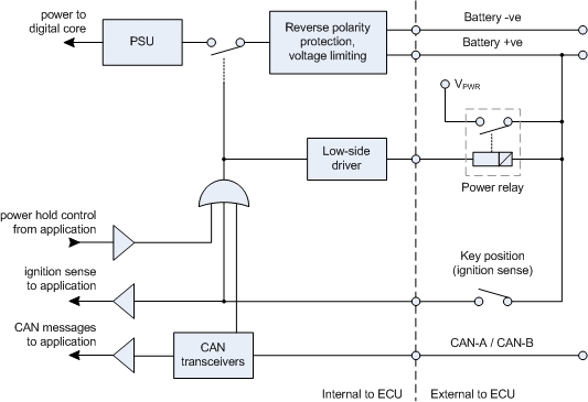
The default build option supports an ignition switch. The ECU powers up when the power supply pins (VPWR Y3, Z2 and Z4) and key position (ignition sense) input (pin Y25) are asserted. The key position voltage threshold, above which the power supply turns on, is nominally 1.7V (worst case, a minimum of 1.1V and a maximum of 2.9V). The key position (pin Y25) can be read as a digital input. The application must debounce the digital input over 200 milliseconds to achieve an accurate reading.
The default build option supports a power relay control driver (pin Z19). When the ECU is powered on, this pin is pulled low by a low-side driver. When the ECU is powered off, the pin is disabled. This pin can be connected to a Power relay as shown in Figure 4.1, “Switching arrangement for main power supply, wake-on-CAN enabled” to create a VPWR supply to external loads which do not have any other high-side supply.
The default build option supports wake-on-CAN. The ECU powers up when the power supply pins are asserted and the ECU receives a message on a wake-on-CAN-enabled CAN bus (see Section 4.4, “ECU power — wake-on-CAN” for more). To fully disable wake-on-CAN, ECUs can be modified with a build option. To partially disable wake-on-CAN, so that an ECU does not power up due to CAN messages but will remain powered when CAN messages are present, VPWR can be used to supply pins Y3, Z2 and Z4 as shown in Figure 4.2, “Switching arrangement for main power supply, wake-on-CAN partially disabled”.
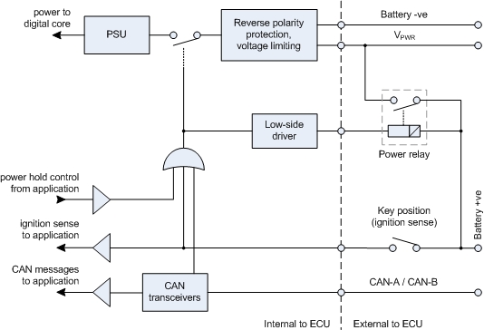
In both switching arrangements shown, the ECU relies on an external power relay to provide a switched high side, VPWR. Connecting actuators directly to low-side outputs from the ECU and battery positive, may result in the ECU generating an incorrect voltage on a high-side pin, or the ECU turning on unexpectedly, or the ECU remaining powered on when the application attempts to shutdown. See Section 4.30, “Digital outputs — high-side to low-side assocations” for details on what outputs to connect to VPWR.
In both switching arrangements shown, the ECU application software can hold power to the ECU after the conditions to power up the ECU no longer exist (e.g., the ignition sense is deasserted or CAN messages are no longer present). This allows, for example, the application to complete non-volatile memory processing. For the ECU to hold power the internal DOT enable-PSU-hold channel needs to be asserted. Setting this internal channel high will hold power when the key position input is opened, setting it low will allow the ECU to power off when the key position input is opened.
Note
The ECU will turn on and assert power hold before the application starts to run. The application must disable power hold by deasserting the internal channel DOT enable-PSU-hold when the conditions to shutdown are satisfied (for instance, the ignition sense input is off and information to store in non-volatile information has been written).
In particular, the ECU may turn on when battery power is first connected. When the application wakes up, the application must determine whether to continue or not, and if not, power down by deasserting the internal channel DOT enable-PSU-hold.
When the ECU is in reprogramming mode, the power hold will automatically be controlled.
If the ignition input is ever enabled, then the power hold is held low for the rest of the power cycle such that the ECU will power down as soon as the ignition is disabled.
If the ignition input is not enabled within a reprogramming power cycle, i.e. The ECU is powered from Wake-on-CAN, then the power hold will remain on for 20 seconds after the last CCP message it receives. This allows the ECU to remain powered while connected to a CCP tool but eventually turn itself off after disconnecting.
See Section 4.64, “System modes” for more information on reprogramming mode.
Some CAN buses (pins Y11, Y12, Y23 and Y24) provide wake-on-CAN functionality. When the ECU power is controlled using CAN messages, the ECU powers up (or wakes) when the ECU senses two bus dominant states of at most 5 microseconds, with the first dominant state followed by a recessive state of at most 5 microseconds (provided the complete dominant-recessive-dominant pattern is completed within at most 2 milliseconds). Generally this pattern is fulfilled by sending a valid CAN message.
When ECU is powered via wake-on-CAN, it is the responsibility of the application to determine how long the ECU should remain on. In order to guarantee that the application is able to run after a wake-on-CAN event, it is recommended that the application initialise the DOT enable-PSU-hold channel to high to keep the ECU powered.
When the application has completed its desired tasks, the internal digital output DOT enable-PSU-hold should be set to low to allow the ECU to shut down. Once both the power-hold output and ignition input are deasserted, the platform will disable the CAN transceivers to cause the ECU to shut down.
Note
If the ECU is initially powered via wake-on-CAN and then the ignition input becomes active while the application is running, the ECU will remain on while the ignition is on even if the power-hold is disabled.
The ECU provides a number of high-side actuator supplies (pins Y1, Y5, Z1 and Z5) to provide switched high-side power to various loads. Supplies on pins Y1 and Y5 are general purpose and controlled as digital outputs (see Section 4.27, “Digital outputs” and Section 4.29, “Digital outputs — high-side” for more). Supplies on pins Z1 and Z5 are specifically intended for use with injector circuits and are described in further detail in Section 4.36, “Digital outputs — injection variants”.
The actuator supply pins Y1 and Y5 must be enabled by initialising the internal digital output DOT reset channel to high. The actuator supply device can be reset to the default state by toggling the DOT reset low for at least 325 ms, while both of the output channels, Y1 and Y5 are also set low.
Note
Severe faults (Monitor (severe short circuit), Monitor (severe short circuit), Monitor (ct), Monitor (ct), Monitor (uv)) related to the actuator supply pins Y1 and Y5 are latched in hardware and cannot be reset or cleared unless the output channels, Y1 and Y5, are set low for at least 325 ms.
The general purpose actuator supplies (pins Y1 and Y5) provide various monitors. Unless specified otherwise, the diagnostic information is sampled at the fastest application task rate of which one of the corresponding diagnostic inputs is read. If the internal digital output DOT reset channel is set to low, then all the diagnostic inputs will read low.
Digital state monitors — The requested drive state monitors (channels Monitor (requested state) and Monitor (requested state)) provide feedback of the output state requested by the application. The output digital monitors (channels Monitor (d) and Monitor (d)) provide feedback of the state actually output by the ASIC.
Fault mode presence monitors — The fault status monitor (channel Monitor (no fault)) is essentially a NOR operation of all other diagnostic monitors. If 0, this indicates that at least one of over-current, over-temperature, output connected to VPWR, severe short-circuit, open-load, over-voltage, or under-voltage is raised. The fail-safe output monitor (channel Monitor (fail-safe disabled)) indicates that the device has gone into fail-safe mode. If 0, this indicates loss of SPI communication or loss of SPI supply voltage.
Over-current trip monitors — The over-current monitors (channels Monitor (ct) and Monitor (ct)) indicate that the corresponding channel's current has gone out side the over-current profile. The over-current profile is exceeded when the current is greater than 70A at any point in time, or greater than 12A for longer than 17.2 milliseconds. Over stressing either actuator supply may reduce the life of the ECU. The actuator supply is considered over stressed if it sustains 10A for more than 50 ms. The application is responsible for ensuring that the outputs are not routinely overstressed.
Short circuit monitors — The short-to-battery monitors (channels Monitor (sb) and Monitor (sb)) indicate that the output pin is shorted to VPWR. This error is detected only while the channel is in the off state. The severe short circuit monitors (channels Monitor (severe short circuit) and Monitor (severe short circuit)) indicates if the output is shorted to ground. If resistance of the load is so low that it is effectively a 1.828 mm (13 AWG) wire less than 170 cm in length, then the output will be immediately tripped off.
Open load monitors — The open-load-off monitors (channels Monitor (off ol) and Monitor (off ol)) indicate that no load is attached when the pin is the off state. The open-load-on monitors (channels Monitor (on ol) and Monitor (on ol)) indicate that no load is attached when the pin is the on state.
Note
The open-load fault can occur unexpectedly. If the current flowing through the high-side is very small, less than 500mA, then the device may detect this as an open circuit fault even if no such fault is present.
Over-temperature warning — The over-temperature warning (channel Monitor (ot warning) indicates that the output is experiencing temperatures that may result in an over-current trip.
Voltage range monitors — The over-voltage monitor (channel Monitor (ov)) indicates that VPWR is above the over-voltage threshold, 39V. The fault remains active until VPWR drops below the over-voltage hysteresis threshold, 37.5V. The output pins will be disabled while this fault is active. The under-voltage monitor (channel Monitor (uv)) indicates that VPWR is below the under-voltage threshold, 6V. The fault remains active while VPWR is below the under-voltage threshold.
Current monitors — The multiplexed current monitors (channels Monitor (c) and Monitor (c)) are cyclically sampled every 150 milliseconds. The current monitors are valid when the outputs are turned on; if one of the actuator power channels is turned off, then the current monitor will not be updated.
The ECU provides a number of sensor power supplies (pins XG2, XH2+Z14, XJ2+Z8 and XK2+Y8) for use with some digital input signals and with ratiometric sensors (see Section 4.12, “Analogue inputs — ratiometric measurement” for more).
Each sensor power supply has a corresponding return sensor ground (pins XG3, XH3+Z15, XJ3+Z9 and XK3+Y9). The return for each sensor power supply is grounded internally to the ECU so that the A/D conversion accuracy can be maintained. The return sensor grounds must not be grounded in the wiring harness.
The sensor power supplies can be individually switched on or off using an internal digital output (for example, see DOT disable to allow the application software to perform intrusive diagnostics on sensors).
WARNING: All voltage references emit a pulse during reset so their values can't be relied on during a reset.
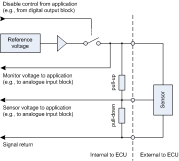
The sensor power supplies (pins XG2, XH2+Z14, XJ2+Z8 and XK2+Y8) include protection circuitry to prevent damage. Protection includes over-current limitation of 400mA at 125°C (nominal, but can be as low as 251mA or as high as 600mA), thermal shutdown by reducing the output current (covering continuous short-to-ground) and protection against reverse polarity (thermal shutdown does not operate during reverse battery). However, a sensor power supply can be damaged by powering into a short-to-battery or short-to-ground.
Protection functions are not designed for continuous repetitive operation, which will reduce the life time of the ECU components.
Each sensor power supply is monitored by an internal analogue input channels (see Monitor (v), Monitor (v), Monitor (v) and Monitor (v)) which can be used to check for electrical faults.
Table 4.3. Sensor supply monitor voltages
| Voltage [a] | Meaning |
|---|---|
| 4.393 < V <= 5.000 | Output shorted to battery when sensor supply enabled or disabled |
| 4.363 < V <= 4.393 | Normal operation when sensor supply enabled |
| 0.000 < V <= 4.363 | Output over-current or shorted to ground when sensor supply enabled |
[a] These voltages are based on absolute A/D counts (referenced to the ECU's internal 5V supply). | |
The analogue inputs (pins XB2, XB3, XC2, XC3, XD1, XD2, XE1, XG1, XJ1, XK1, Y19, Y31, Z16, Z20, Z21, Z24, Z25, Z26, Z27, Z28, Z32, Z33, Z40, Z44, Z45, Z50, Z51 and Z52) sample voltage with varying resolution and range. See the pin information for more details. Some of the analogue inputs have additional characteristics, as detailed in the following sections.
Note
If any of the pins XL1, XL4, XM1, XM2, XM3, XM4, Y6, Y18, Y29, Y30, Y41, Y42 and Y53 are not being used as digital outputs then it is possible for them to be used as analogue inputs with a nominal range of 0V to 38.33V and bias of 4V. Providing the output transistor is switched off, the pin can be driven by an external source and pin's voltage monitor will reflect the actual voltage on the pin.
The ECU sensor supply arrangement is shown in Figure 4.4, “VREF arrangement”. The figure shows the relationship between the internal 5V reference supply and ground, the external sensor supply and ground, and the analogue inputs.
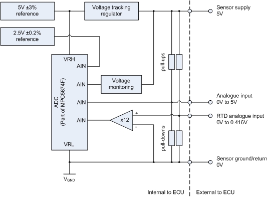
The internal low precision 5V reference supplies the reference pin on the ADC. A high precision 2.5V reference can be read on a direct (unscaled) ADC channel. This can be used to calculate the true value of the 5V reference and subsequently used to improve accuracy on all other channels (see Section 4.12, “Analogue inputs — ratiometric measurement”).
The exact supply voltage being produced can be monitored on a direct (scaled) ADC channel. The sensor ground is a nominal 0V, but may be slightly above this due to voltage drop across the protection device.
There are three sensor supplies relevant to analogue inputs (only one is shown in Figure 4.4, “VREF arrangement”. For ratiometric analogue inputs, those sensors which generate a voltage proportional to the supply voltage, it is preferable to attach the sensor to an analogue input pin which a pull-up to the same sensor supply. Then if a sensor becomes disconnected, the analogue input will default to a known out of range value.
For example, the following are two examples of potential problems when a sensor is supplied from VREFA but its input is pulled up to VREFB.
An external fault on the VREFA output pulls its voltage down to some mid range value, say 2V, and then the sensor becomes disconnected — there is no way of knowing if the value of 2V read from the sensor input is the actual output of the sensor or the effect of the pull up to VREFB.
A short-to-battery occurs on VREFB, the sensor is now being pulled up to 12V or 24V instead of 5V, and more current is flowing in the pull up. This excessive current may be enough to overcome the output of the sensor and lead to a false high reading.
The analogue inputs are grouped by pull-up resistors to sensor supplies as detailed in Table 4.4, “Association of sensor supplies and analogue inputs”.
Ratiometric sensors are read in as a ratio between the sensor and reference voltages (Vsens/Vref). Correction is only required on channels for which an absolute voltage measurement is required. Correction is not required for sensors supplied from the 5V sensor supply and which produce an output that is ratiometric to the supply.
To read a variable sensor which is an absolute referenced sensor (Vsens/Vabs) the Vref for the ADC requires correction:
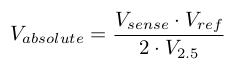
Where Vsense is the A/D conversion for an external pin, Vref is the A/D conversion for the corresponding sensor supply voltage monitor (one of Monitor (v), Monitor (v), Monitor (v), Monitor (v)), and V2.5 is the A/D conversion for internal channel AIN +2.5V.
The Resistance Temperature Detector (RTD) inputs (pins XD1, Z26, Z40 and Z44) provide support for PT-100 like sensors, a platinum RTD that measures 100R at 0°C. The RTD inputs provide an accuracy of ±10°C and resolution of 1°C over the temperature range -40°C to +900°C. The input pins have an amplifier to increase the sensitivity for the RTD's low-voltage signal. The conversion from input voltage, VADC, to temperature TSENSOR, is nearly linear, but is better represented in table form.
Table 4.5. RTD temperature conversion
| TSENSOR °C | RSENSOR Ohms | VADC mV | TSENSOR °C | RSENSOR Ohms | VADC mV |
|---|---|---|---|---|---|
| -50 | 80 | 342 | 40 | 116 | 491 |
| -45 | 82 | 351 | 45 | 117 | 499 |
| -40 | 84 | 359 | 50 | 119 | 507 |
| -35 | 86 | 367 | 55 | 121 | 515 |
| -30 | 88 | 376 | 60 | 123 | 524 |
| -25 | 90 | 384 | 65 | 125 | 532 |
| -20 | 92 | 392 | 70 | 127 | 540 |
| -15 | 94 | 401 | 75 | 129 | 548 |
| -10 | 96 | 409 | 80 | 131 | 556 |
| -5 | 98 | 417 | 85 | 133 | 564 |
| 0 | 100 | 426 | 90 | 135 | 572 |
| 5 | 102 | 434 | 95 | 137 | 580 |
| 10 | 104 | 442 | 100 | 139 | 588 |
| 15 | 106 | 450 | 105 | 140 | 596 |
| 20 | 108 | 458 | 110 | 142 | 604 |
| 25 | 110 | 467 | 150 | 157 | 667 |
| 30 | 112 | 475 | 200 | 176 | 744 |
| 35 | 114 | 483 | |||
The thermistor inputs (pins XC3, XG1, Y19, Z45 and Z51) have a standard circuit with pull-up bias, with an accuracy of ±2°C and resolution of 1°C over the temperature range -40°C to +150°C. The use of a particular thermistor may require implementing a build option to ensure the sensitivity of the circuit to the temperature of interest.
The ECU has an internal thermistor temperature sensor. The conversion from input voltage, VADC, to temperature, TSENSOR, is non-linear. Table 4.6, “Internal temperature conversion” provides nominal, median values; the minimum and maximum are within ±10% from -40°C and up, and ±5% above 95°C.
Table 4.6. Internal temperature conversion
| TSENSOR °C | VADC V | TSENSOR °C | VADC V |
|---|---|---|---|
| -55 | 0.0256 | 50 | 1.8388 |
| -50 | 0.0366 | 55 | 1.9267 |
| -45 | 0.0525 | 60 | 2.0037 |
| -40 | 0.0720 | 65 | 2.0708 |
| -35 | 0.0989 | 70 | 2.1282 |
| -30 | 0.1343 | 75 | 2.1795 |
| -25 | 0.1783 | 80 | 2.2222 |
| -20 | 0.2332 | 85 | 2.2601 |
| -15 | 0.3016 | 90 | 2.2918 |
| -10 | 0.3834 | 95 | 2.3187 |
| -5 | 0.4774 | 100 | 2.3431 |
| 0 | 0.5861 | 105 | 2.3626 |
| 5 | 0.7070 | 110 | 2.3797 |
| 10 | 0.8364 | 115 | 2.3956 |
| 15 | 0.9719 | 120 | 2.4078 |
| 20 | 1.1111 | 125 | 2.4188 |
| 25 | 1.2503 | 130 | 2.4286 |
| 30 | 1.3846 | 135 | 2.4371 |
| 35 | 1.5128 | 140 | 2.4444 |
| 40 | 1.6325 | 145 | 2.4505 |
| 45 | 1.7411 | 150 | 2.4554 |
The ECU provides pedal position inputs (pins Z27 and Z28) and throttle position inputs (pins Z20 and Z21) which are available to the primary and secondary processor (see Section 4.54, “Secondary processor” for details on the secondary processor). The intent is two fold:
Redundant sensors — The two pedal position sensors should have different offsets and gains so that the application can redundantly check the position voltages correlate. Similarly for the throttle sensors.
Cross monitoring — Where both processors can derive information based on the same pedal position, and cross check the other processor for expected behaviour. Similarly for the throttle sensors.
There are two further throttle position inputs (pins XC2 and XD2) which are available to the primary processor only.
The crank input (pins Y32+Y33) provides input circuitry suitable for a differential or single-ended Variable Reluctance sensor. A VR sensor produces a quasi sine wave output in which the zero-crossing point (in one direction) indicates the center of a toothed wheel. The conditioning circuitry amplifies the VR signal, determines an adaptive threshold used in noise reduction, and determines zero crossings representing the center of teeth.
Once the VR input signal voltage rises above an adaptive threshold, the zero crossing comparator is armed. Arming the comparator this way provides robust noise immunity to the input VR signal, preventing false triggers from occurring due to a broken tooth or an off-center tooth wheel.
The peak threshold level is set to a third of the peak of the previous cycle of the input VR signal. As the sensor signal peak voltage rises, the adaptive peak threshold voltage also increases by the same ratio. Similarly as the signal peak voltage falls. If the input signal voltage remains lower than the adaptive peak threshold for more than 85 milliseconds, an internal watchdog timer drops the threshold level to a default minimum threshold. This ensures pulse recognition recovers even in the presence of intermittent sensor connection.
Once armed, the zero crossing detection logic generates a digital edge on the next falling (positive-to-negative) zero crossing point of the VR signal. The zero-voltage level of the VR sensor signal corresponds to the center of the tooth and is the most reliable marker for position/angle-sensing applications.
The VR input circuitry introduces a phase offset as an artifact of signal filtering. The phase shift causes the digital edge representing the tooth center to occur some time after the actual tooth center. The time between the digital tooth edge and the actual tooth center increases as the frequency of the input signal increases. At 10,000 RPM that delay is approximately half a degree of crank angle.
The peak-to-peak voltage range for each VR input varies with temperature. The following voltage limits are with full power loading of the outputs. The voltage limits will be higher with lighter load conditions.
Table 4.7. VR input voltage range
| Operating temperature | Input voltage range |
|---|---|
| -40°C to +85°C | ±100mV to ±200V peak sine wave voltage |
| -40°C to 105°C | ±100mV to ±157V peak sine wave voltage |
Pins Y32+Y33 are suitable for a differential VR sensor. Pin Y32 is suitable for a single-ended VR sensor when pin Y33 is connected to ground. A single-ended VR sensor may benefit from connecting pin Y33 to ground near the sensor. Connecting Y33 to chassis ground may introduce detrimental noise or voltage shift present on the chassis.
When using a VR sensor for crank, the application must drive the internal digital output DOT select Hall-effect for pins Y32+Y33 low. The crank input can be connected to a Hall-effect sensor, see Section 4.23, “Digital inputs — crank and cam, Hall-effect” for more.
Note
The M670 hardware is optimised for Hall-effect sensors as the standard build option. When using a VR crank sensor, the M670 should be ordered with the VR crank sensor build option.
The ECU uses the HIP-9011 device for processing the signal from a knock sensor. It contains one such device, which can be configured to select from either of two possible differential signal sources, pins Z48+Z49 or pins Y51+Y52.
A simplified view of the knock signal processing stages is given in the following block diagram:

The knock signal to process is first selected from two differential inputs. The device responsible for detecting knock can process just one sensor at a time.
The knock signal is then passed through a 3rd order anti-aliasing filter. This filter is required to have no more than 1dB attenuation at 20kHz (highest frequency of interest) and a minimum attenuation of 10dB at 180kHz.
The knock signal is then passed through a gain stage to compensate knock energies if needed.
The knock signal is then passed through a band-pass filter to detect the frequencies of interest. The filter frequency is established by the characteristics of the particular engine and transducer.
The knock signal is then passed through a full wave rectifier before being passed into an integrator stage, the output of which can be monitored for knock. Integration is towards the positive supply when a knock signal is present.
The result of the knock processing can be measured through the channels associated with either the Z48+Z49 or Y51+Y52 channel as appropriate, using the dedicated knock-processing application interface as described in detail in the User Guide. The interface also allows the band-pass filter frequency, gain and integration time constant to be configured by the application.
Single-ended knock sensors may be used with the M670. For single ended knock sensors, the signal wire can be connected to Z49 or Y52. Pins Z48 and Y51 should be left unconnected.
The ECU uses multiplexers to accomodate the large quantity of diagnostic analogue signals. The multiplexers extend the number of analogue input pins on the primary processor. Whilst scanning the analogue inputs, the processor selects a multiplexer device and channel, lets the selection settle, then samples the input.
One multiplexer device is assigned to the following channels: AIN +12.5V, XC3, Monitor (v) (for pin X11), Monitor (v) (for pin Y18) and Monitor (v) (for pin Y29).
The other multiplexer device is assigned to the following channels: AIN +5.0V, AIN PCB-temp, Monitor (v) (for pin XM1), Monitor (v) (for pin Y41) and Monitor (v) (for pin Y53).
The multplexed inputs are less accurate than others. The inaccuracy is caused by a leakage current through the multiplexer, showing up as a voltage offset at the A/D converter. Current leakage will vary part-to-part, over temperature and over life.
The analogue outputs (pins XD4, XL2, Y7, Y10, Y13, Y16, Y17 and Z7) drive a constant current into an external load.
The constant current outputs (pins XD4, XL2, Y7, Y10, Y13, Y16, Y17 and Z7) are a collection of digital low-side outputs driven by a programmable current control pre-driver. With a low-side output, the ECU switches the output pin to ground, the load is connected to the output pin and VPWR. These outputs are designed to drive proportional solenoid valves.
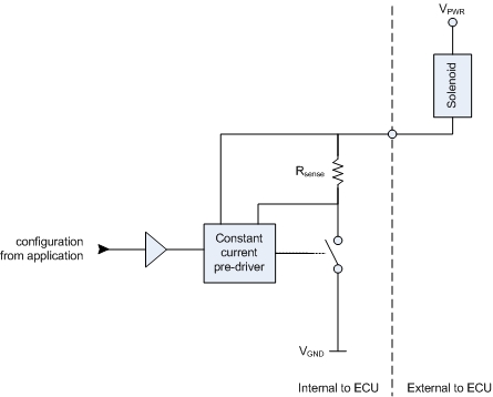
- Closed loop control
The pre-driver switches an output to ground at a constant frequency with a variable duty cycle. The desired set point is maintained by a PI control loop within the pre-driver that continuously adjusts the duty cycle. The PI controller gain values KP and KI are configurable by the application and are independently set for each output (see the Sim-API pax_CcConfigTle8242 block and C-API
pax_cc_config_tle8242()function).Care must be taken in selecting appropriate KP and KI values to prevent damage to the solenoids. If the application does not provide KP and KI values, then the platform will use default values of zero. When KP and KI are set to zero, the duty cycle will remain at zero and the output will not sink current. The following diagram describes the control loop.
- Triangular dither
Dither is useful in some applications to reduce mechanical hysteresis and stiction.
A triangular dither waveform can be superimposed on the current set point for each constant current output. The dither waveform is configured by the application independently for each output.
- Automatic zeroing
The constant current pre-driver supports an auto-zero feature for each output (see the Sim-API pax_CcAutozeroTle8242 block and C-API
pax_cc_autozero_tle8242()function). The auto-zero sequences can be run when the current set point is zero. The auto-zero sequence observes the measurement offset and stores the result internally. The offset is automatically applied to the current measurement until the device is reset or the auto-zero sequence is repeated. The device is capable of retaining offsets for each channel, but can only carry out the offset measurements for one channel at a time.The application is responsible for setting the output set point to zero, allowing settle time, and initiating the auto-zero sequence. Since the auto-zero sequence can only be executed for one output at a time, the application is also responsible for sequentially zeroing the desired outputs.
- Current monitoring
The constant current output pre-driver is capable of reporting current measurement for one output at any given time (see the Sim-API pax_CcReadCurrentTle8242 block and the C-API
pax_cc_select_meas_chan_tle8242()andpax_cc_read_meas_chan_tle8242()functions). The pre-driver must continuously measure current for use in the control loop for each output but this information is not actively reported to the primary processor. Application interfaces are provided to select an output for current measurement and retrieve the current measurement data. If the output is configured with dither, then the measurement will be updated at the end of a complete dither cycle and minimum, maximum, and average current measurements will be reported for the dither cycle.- Driver protection
Each constant current pin individually detects short-to-battery, short-to-ground and open-load fault conditions. See Section 4.33, “Digital outputs — monitors (conditioned)” for further details.
- Phase synchronisation
The PWM control signals of each constant current output channel can be synchronised with the internal DOT sync-phase digital output. The delay between the rising edge of the phase sync digital output and the PWM signal is individually configured for each output.
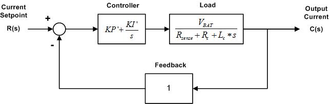
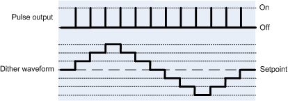
Note
If any of the pins XD4, XL2, Y7, Y10, Y13, Y16, Y17 and Z7 are not being used as constant current outputs
then it is possible for them to be used as digital PWM outputs. When used in PWM mode,
do not configure the pin for constant current mode using either the Sim-API
pax_CcConfigTle8242 block or C-API
pax_cc_config_tle8242() function.
Warning
Connecting any of the constant current outputs directly to Battery +ve will greatly increase quiescent current and may not allow the ECU to turn off.
The digital inputs (pins XF3, XG4, XH4, Y14, Y15, Y20, Y21, Y32+Y33, Y34, Y43, Y46, Z12 and Z13) sample a digital state, allowing the measurement of switches or pulsing inputs. See the pin information for more details. Some of the digital inputs have additional characteristics, as detailed in the following sections.
The inputs are not inverted. Below 1.6V, the input reads low; above 3.6V the input reads high.
To support a variety of sensors, the ECU is pre-populated with a default selection of inputs with varying voltage thresholds and pull strengths. In some cases, the default selection will not meet the requirements of all customers. To help, Pi can modify the ECU PCB component population to adjust these characteristics as build options. Contact Pi for further information.
Note
The external signals are all low pass filtered to prevent signals of excessive frequency from tying up the target processor.
The crank and cam inputs (pins XG4, XH4, Y14, Y15 and Y32) provide input circuitry suitable for Hall-effect sensors. A Hall-effect sensor produces a square wave output between VGND and VPWR, in which the change of state (in one direction) indicates the start of a crank or cam trigger wheel tooth.
The input circuitry voltage threshold is fixed at a little over 2V. The falling edge provides the tooth indication by default.
Some Hall-effect sensors may benefit from an external pull up resistor. If the sensor is an open drain type that needs to operate above some frequency (1kHz for cam inputs, 30kHz for crank inputs), it would benefit from a change to a pull value or a change in ESD capacitor. Pi can accomodate this through a build option.
When using a Hall-effect sensor for Y32+Y33, the application must drive the internal digital output DOT select Hall-effect high. The crank input can be connected to a VR sensor, see Section 4.17, “Analogue inputs — crank, VR” for more.
Note
The crank sensor inputs (pins Y32+Y33) are inverted in hardware, but the OpenECU developer software is configured for the polarity of the microcontroller pin, not the connector pin. Therefore, when configuring your crank wheel you must use falling-edge detection when you would like to use the rising edge of your sensor. Likewise, select rising-edge detection when you would like to use the falling edge of your sensor.
Note
When using a Hall-effect sensor, the falling edge of the sensor will provide more accurate and repeatable edge detection. Since the crank sensor signal is inverted in hardware, you should configure your crank wheel to use rising edge detection for the most accurate edge detection. The default edge detection is falling-edge.
The ECU measures a signal frequency and duty cycle by capturing the time of the signal's filtered digital edges arriving at the processor. The time between similar edges gives the cycle period of the signal, and the inverse of the cycle period gives the frequency of the signal. The time between opposing edges gives the on and off periods, and the ratio of either the on or off period to the cycle period gives the corresponding on or off duty cycle.
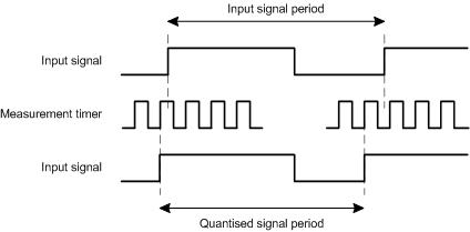
The filtered digital edges for each input pin are captured relative to a digital timer. The digital timer has two properties that affect the measurable range of frequency.
- Timer frequency
Each timer counts at a fixed frequency. When the state of the filtered digital signal changes (an edge occurs), the timer count is captured. If the state of the filtered digital signal changes between timer counts, then the measured frequency is quantised and less accurate. The resolution of the measured frequency can be calculated as:
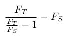
where FT is the timer frequency and FS is the signal frequency.
Note that as the signal frequency increases, the measured resolution decreases. For instance, with a 1000 Hz input signal and 4 MHz timer, results in a resolution of approximately 0.25 Hz. A 10000 Hz input signal and 4 MHz time, results in a resolution of appoximately 25 Hz.
Pins XF3, XG4, XH4, Y14, Y15, Y20, Y21, Y32+Y33, Y34, Y43, Y46, Z12 and Z13 use a 4.125 MHz timer for frequency inputs, and pins Y20, Y21 and Y43 can be adjusted to use a 8.25 MHz or 16.5 MHz timer.
- Timer size
Each timer is free running, meaning the timer is incremented modulo N, where N is the size of the timer. The larger N, the longer a signal cycle period that can be measured. Thus the size of the timer limits the lowest frequency that can be measured. The user guide documentation indicates measurement frequency ranges.
The M670 decodes quadrature inputs using two timer/capture devices on the primary microcontroller. To properly decode the quadrature inputs, both quadrature channels must go to the same microcontroller device.
The following inputs are routed to device 0: XF3, Y14, and Y32.
The following inputs are routed to device 1: XG4, XH4, and Y15.
Pins XA1, XA2, XA3, XA4, XF3, XF3, XG4 and XH4 provide support for SENT sensors. To use the SENT channels, see the C-API or Sim-API User Guide for further details.
The digital outputs (pins XB1, XE3, XL1, XL3, XL4, XM1, XM4, Y6, Y18, Y29, Y30, Y37, Y38, Y39, Y40, Y41, Y42, Y44, Y45, Y49, Y50, Y53, Z6, Z17, Z18, Z29, Z30, Z31, Z36, Z37, Z38, Z39, Z41, Z42, Z43 and Z53) are a collection of low-side and high-side drivers, and described in further detail in the following sections.
When the application starts, the application must enable various devices to achieve full functionality.
Each set of banked outputs on pins Y18, Z1, Z6, Z18, Z30 and Z42 (bank A) and Y53, Z5, Z17, Z29, Z41 and Z53 (bank B) has an internal digital output (see DOT enable for bank A). Each digital output must be asserted to enable injections on each respective bank.
The same set of banked outputs have fault detection for loss of clock, short-to-battery, short-to-ground, and boost overcurrent which will disable injections. Each bank has internal digital outputs (see DOT reset clock bank A and DOT reset-fault bank A) These digital outputs must be actioned twice over consecutive application loops, to enable injections on each respective bank.
For M670B and M670N variants, the same set of banked outputs have software configurable waveforms, see Section 4.35, “Digital outputs — waveform control”. Each output must be configured to enable injections.
The low-side outputs and constant current outputs have a combined internal digital output named DOT enable. The digital output must be asserted to enable these outputs.
Warning
If the application does not enable these low-side outputs, then the flash code output (pin Y28) will not work during application mode.
With the low-side outputs (pins XB1, XD4, XE3, XL1, XL2, XL3, XM1, Y6, Y7, Y10, Y13, Y16, Y17, Y18, Y29, Y37, Y38, Y39, Y40, Y41, Y44, Y45, Y49, Y50, Y53, Z6, Z7, Z17, Z18, Z19, Z29, Z30, Z31, Z36, Z37, Z38, Z39, Z41, Z42, Z43 and Z53) the ECU switches the output pin to ground, the actuator is connected to the output pin and either to one of the ECU's high-side actuator pins, or to VPWR.
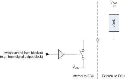
The lower current low-side outputs (pins XB1, XE3, XL3, Y28, Z19, Z31, Z36, Z37, Z38, Z39 and Z43) are protected against over-voltage up to 24V. These outputs have recirculation diodes to VPWR and can drive inductive loads at a maximum rate of 100 Hz.
Warning
A subset of the lower current low-side outputs (pins XB1, XL3, Y28, Z31, Z36, Z37, Z38, Z39 and Z43) are vulnerable to short-to-battery in 24V systems. Over-current fault status is one symptom of a battery short. The application must avoid activating these low-side outputs once a battery short is known.
The higher current low-side outputs (pins XL1, XM1, Y6, Y18, Y29, Y41 and Y53) are capable of driving actuators of 10 mH up to 1 kHz PWM, of 1mH between 1 kHz to 5 kHz, and of 500 uH between 5 kHz and 10 kHz.
The low-side “smart ignition” outputs (pins Y37, Y38, Y39, Y40, Y44, Y45, Y49 and Y50) are described in detail in Section 4.42, “Digital outputs — ignition”.
Each low-side output has an associated high-side output. It is important to adhere to the association otherwise the ECU may generate an incorrect voltage on a high-side pin, or the ECU may turn on unexpectedly, or the ECU may remain powered on when the application attempts to shutdown. See Section 4.30, “Digital outputs — high-side to low-side assocations” for details.
With the general high-side outputs (pins Y1 and Y5), the ECU switches the output pin to VPWR, the actuator is connected to the output pin and VGND.
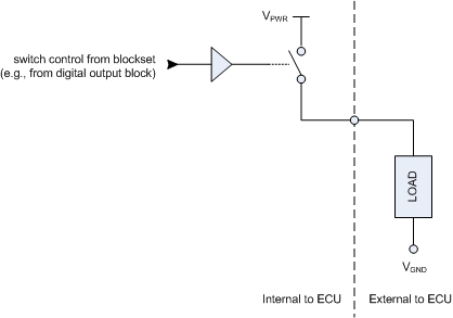
The high-side supply pins Y1 and Y5 must be enabled by driving the internal digital output DOT reset channel high. The device controlling the high-side supply pins can be reset to the default state by toggling the DOT reset low for at least 325 ms, while both of the output channels, Y1 and Y5, are also set low.
Each low-side output has an associated high-side output. It is important to adhere to the association otherwise the ECU may generate an incorrect voltage on a high-side pin, or the ECU may turn on unexpectedly, or the ECU may remain powered on when the application attempts to shutdown. See Section 4.30, “Digital outputs — high-side to low-side assocations” for details.
There are two further high side outputs (pins Z1 and Z5) dedicated to the injector outputs (pins Z6, Z17, Z18, Z29, Z30, Z41, Z42 and Z53). Further details can be found in section Section 4.36, “Digital outputs — injection variants”.
Due to internal circuitry, such as clamping and recirculation diodes, heat dissipation and safety, low-side outputs must be connected to the following high-side outputs:
Warning
Failure to adhere to the high and low side arrangement, may result in the incorrect voltage on a high-side pin, or the ECU turning on, or the ECU remaining powered on when the application attempts to shutdown.
The digital outputs contain internal monitoring circuitry that provides diagnostic information (see Section 4.32, “Digital outputs — monitors (unconditioned)” and Section 4.33, “Digital outputs — monitors (conditioned)”). As a consequence a small leakage current will flow through the actuator when the output driver is turned off. Refer to Table 4.9, “Digital output leakage current (room temperature)” for typical leakage currents at specified operating voltages. When the ECU is turned off, the leakage current will be much less.
Table 4.9. Digital output leakage current (room temperature)
|
Output
type |
Supply voltage
V |
Typical leakage current
mA |
|---|---|---|
| H-bridge, 4A, 6A/4A and 8A outputs | 12 | 0.6mA |
| H-bridge, 4A, 6A/4A and 8A outputs | 24 | 1.3mA |
| 0.2A and 0.5A outputs | 12 | 0.012mA |
| Spark outputs | 12 | 0.128mA |
| Spark outputs | 24 | 0.271mA |
| Constant current outputs | 12 | 0.225mA |
| Constant current outputs | 24 | 0.225mA |
| Injector outputs (set to internal biasing) | 12 | 13mA |
The low-side and high-side digital outputs contain a mixture of monitoring circuitry that provides unconditioned diagnostic information that can be used for electrical diagnostics, such as current, state and voltage monitors. These monitors are available to the application as individual analogue inputs and digital inputs.
Current — current monitors are provided for pins XL4, XM4, Y1, Y5, Y30 and Y42. The monitors provide a current reading for actuator supplies and H-bridge functions.
Current-trip — current-trip monitors are provided for pins XB1, XG2, XH2+Z14, XJ2+Z8, XK2+Y8, XL1, XL3, XL4+XM4, XM1, XM2+XM3, Y1, Y5, Y6, Y18, Y28, Y29, Y30+Y42, Y37, Y38, Y39, Y40, Y41, Y44, Y45, Y49, Y50, Y53, Z1+Z5, Z31, Z36, Z37, Z38, Z39 and Z43. When any of these digital outputs goes over-current, the output is latched off and the current-trip is asserted (active low). The application must clear the latch before the output can be turned on again.
Drive state — digital output state monitors are provided for pins Y1 and Y5. Drive state monitors provide the driven state, on or off, of an output pin or an internal function of the ECU.
Requested drive state — digital output requested state monitors are provided for pins XB1, XL3, Y1, Y5, Y28, Z31, Z36, Z37, Z38, Z39 and Z43. Requested state monitors provide the commanded driven state, on or off, of an output pin or an internal function of the ECU.
Voltage — voltage monitors are provided for pins , XG2, XH2+Z14, XJ2+Z8, XK2+Y8, XL1, XL4, XM1, XM2, XM3, XM4, Y3+Z2+Z4, Y6, Y18, Y29, Y30, Y41, Y42 and Y53. The monitors provide a voltage reading of ECU supply, sensor supply, injector boost power supply and H-bridge circuits.
Note
If any of the pins XL1, XL4, XM1, XM2, XM3, XM4, Y6, Y18, Y29, Y30, Y41, Y42 and Y53 are not being used as digital outputs then it is possible for them to be used as analogue inputs with a nominal range of 0V to 38.33V and bias of 4V. Providing the output transistor is switched off, the pin can be driven by an external source and pin's voltage monitor will reflect the actual voltage on the pin.
These monitors can be used by the application to determine electrical faults. For instance, if a digital output is turned on but the corresponding state monitor reads off, then there is likely a short or open in the circuit.
Some digital outputs are driven using integrated devices which provide conditioned electrical diagnostics. The results of these diagnostics, such as short-to-ground, are available to the application as individual digital inputs.
The platform samples diagnostic monitors in groups. If a monitor is asserted, then the corresponding digital input is latched until read by the application. If a monitor is not asserted, then the corresponding digital input is not overwritten. When the application reads one of the digital inputs, the monitor state is provided to the application and the latch cleared. This latching technique allows each diagnostic monitor in a group to be read at different application rates.
- Integrated circuit faults
Some general faults are reported by the integrated circuits. These faults describe the state of the integrated circuit and may affect one or more of the output pins that are driven by the integrated circuit.
Under-voltage VCC (Monitor VCC UV) and Under-voltage VDD (Monitor VDD UV) — An under-voltage fault will be set if the IC detects an under-voltage on the internal 5V power supply. Applicable to pins XB1, XL3, Y28, Z31, Z36, Z37, Z38, Z39 and Z43.
Reset monitor (Monitor reset) — Indicates that the IC has been reset. Applicable to pins XD4, XL2, Y7, Y10, Y13, Y16, Y17 and Z7. Unexpected resets of this IC will result in a loss of any previously zeroed measurement offsets.
Enable monitor (Monitor enable) — Indicates that the IC enable pin was low. Applicable to pins XD4, XL2, Y7, Y10, Y13, Y16, Y17 and Z7. The enable pin should only be low following a reset of the ECU. In any other event, this may indicate an under-voltage on the internal 5V supply.
Fault present (Monitor fault) — Indicates that at least one output is faulted. Applicable to pins XD4, XL2, Y7, Y10, Y13, Y16, Y17 and Z7. Unlike the detailed fault data, this is a physical digital input to the primary processor.
- Fault filter time
The fault filter time TFLT for pins XD4, XL2, Y7, Y10, Y13, Y16, Y17 and Z7 is 11.6 microseconds. The fault filter time for pins XB1, XL3, Y28, Z31, Z36, Z37, Z38, Z39 and Z43 is 150 microseconds.
- Low-side output diagnostics
Short-to-battery faults for low-side outputs can be detected when the transistor gate is in the on (closed) state. If a short is detected, then the output will be turned off to prevent damage to the hardware. Pins XD4, XL2, Y7, Y10, Y13, Y16, Y17 and Z7 will return to normal operation after 240 PWM periods have elapsed. Pins XB1, XL3, Y28, Z31, Z36, Z37, Z38, Z39 and Z43 will return to normal operation as soon as the fault information has been made available to the application.
Short-to-ground and open-load gate-off faults for low-side outputs can be detected when the transistor gate is in the off (open) state. If both short-to-ground and open-load gate-off diagnostics are available, then the fault condition is differentiated with a bias voltage. The output must be turned off and allowed to settle to correctly evaluate the fault condition once either fault is detected.
Open-load gate-on diagnostics are only applicable to constant current outputs (pins XD4, XL2, Y7, Y10, Y13, Y16, Y17 and Z7) that are configured in constant current mode. Open-load gate-on faults are detected by counting the number of PWM periods during which the output duty cycle is at 100%. If 64 consecutive PWM periods are observed with a 100% duty cycle, then the fault becomes active.
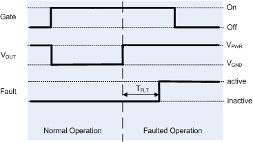
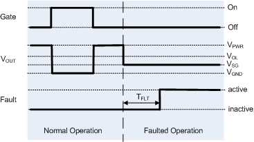
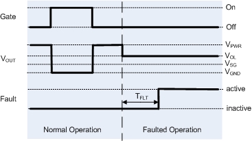
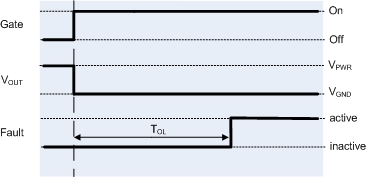
Some digital outputs (pins XB1, XG2, XH2+Z14, XJ2+Z8, XK2+Y8, XL1, XL3, XL4+XM4, XM1, XM2+XM3, Y1, Y5, Y6, Y18, Y28, Y29, Y30+Y42, Y37, Y38, Y39, Y40, Y41, Y44, Y45, Y49, Y50, Y53, Z31, Z36, Z37, Z38, Z39 and Z43) can be monitored for over-current events. The over-current trip state of an output pin is monitored using a corresponding internal over-current monitor channel. In normal operation the internal over-current trip channel will be one. If the output channel experiences an over-current, the output channel will be forced off by the ECU and the over-current trip channel will read low.
The over-current trip latch can be cleared and the tripped outputs enabled by the pss_OvercurTripReset Simulink block or by calling the pss_overcur_trip_reset() C-API function.
Note
To help component heat dissipation and to help prevent component stress, the platform software ensures there is at least 50ms between each request to clear the over-current trip latches.
The ECU provides control over the current and voltage waveform for various outputs (pins Y18, Y53, Z1, Z5, Z6, Z17, Z18, Z29, Z30, Z41, Z42 and Z53). The controlling output pulse, from a digital output or PWM output, gives the overall pulse width, T5. The width is split into three distinct current hold stages:
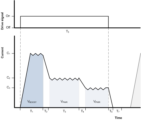
The desired hold current for a stage is specified by Cn. For each stage, the application can select between VPWR or VBOOST, where VBOOST can be controlled to an application set point between 45V and 65V. The higher boost voltage is typically used to energise a coil quickly, thus providing fine control over short digital pulses.
Note
The switching strategy used to maintain the hold current (Cn) uses the nominal value of each component in the measurement circuitry to determine the switching thresholds. Therefore, the actual hold currents may vary slightly from the set current. If your application requires the switching thresholds to be set differently, Contact Pi for further information.
Each stage is split into an on and a switch part. The on part attempts to drive the actuator to a hold current for a time defined by the application before switching to the next stage (the width of the last stage is controlled by T5). A minimum time between pulses must be observed by the application, T7.
The application can select two stage boosted operation:
or apply VBOOST as the second stage (e.g., to pre-energise a solenoid for a more robust action):
In the previous examples, each stage holds the current. The M670 also supports an immediate switch to the next phase when the desired current is reached.
In these cases, the application specified time for the stage is used as a timeout when the desired current can never be reached.
The M670 supports non-boosted operation:
and supports saturating actuators that require a single stage:
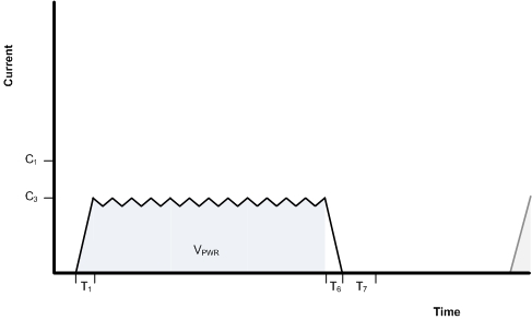
Different ECU variants support different injector types as build options:
| ECU | Build option |
|---|---|
| M670B |
Non-overlapping, boosted and non-boosted, peak and hold solenoid injectors.
Covered by Section 4.37, “Digital outputs — injection”, Section 4.38, “Digital outputs — injection driver protection” and Section 4.39, “Digital outputs — injection monitors”). |
| M670N |
Overlapping non-boosted peak and hold solenoid injectors.
Section 4.40, “Digital outputs — injection variant, M670N” describes the differences between the M670B and M670N. |
| M670S |
Overlapping saturating solenoid injectors.
Section 4.41, “Digital outputs — injection variant, M670S” describes the differences between the M670B and M670S. |
Table 4.10, “Differences between the M670B, M670N and M670S variants” details the differences between the M670B, M670N and M670S variants. The only differences relate to injector channels. All other channels are the same across variants.
Table 4.10. Differences between the M670B, M670N and M670S variants
| Pins |
Boosted peak and hold
[a]
M670B |
Non-boosted peak and hold
M670N |
Saturating
M670S |
|---|---|---|---|
|
Z6
Z17 |
– Current controlled PWM with boost voltage drive
– Z6, Z18, Z30, Z42 driven from injector high-side Z1 – Z17, Z29, Z41, Z53 driven from injector high-side Z5 – 65V boost (up to 120W capable), 25A peak, 15A hold maximum controlled current – 60A drive-from-boost over-current trip on the high-sides – 30A drive-from-battery over-current trip on the high-sides – Each bank of four injector may only drive one injector at a time – Each bank may overlap injector drive with the other bank | Not connected, use pins Y18 and Y53 instead |
– Saturating (non-current controlled), PWM control
– Z6, Z18, Z30, Z42 driven from injector high-side Z1 – Z17, Z29, Z41, Z53 driven from injector high-side Z5 – 3A per channel nominal current capability – 6A shared over-current trip on each pair of channels – 30A over-current trip on the high-side outputs – All injector channels may overlap |
|
Z18
Z30 Z42 Z29 Z41 Z53 |
– Current controlled, PWM control
– 15A maximum controlled current – Z18, Z30, Z42 driven from injector high-side Z1 – Z29, Z41, Z53 driven from injector high-side Z5 – 30A over-current trip on the high-side outputs – All injector channels may overlap | ||
|
Y18
Y53 |
– Current controlled, PWM control
– 6A peak, 4A hold maximum controlled current – Driven from general high-sides Y1 and Y5 respectively – 7.5A low-side over-current trip – Both channels may overlap |
– Current controlled, PWM control
– 6A peak, 4A hold maximum controlled current – Driven from general high-sides Y1 and Y5 respectively – 7.5A low-side over-current trip – 30A over-current trip on the high-side outputs – All injector channels may overlap – Not separately available |
– Current controlled, PWM control
– 6A peak, 4A hold maximum controlled current – Driven from general high-sides Y1 and Y5 respectively – 7.5A low-side over-current trip – Both channels may overlap |
[a] Note: injector drive profiles must be set up with some drive-from-boost time. A M670B should not be used if application injectors do not drive from boost. | |||
The injector control pins (Y18, Y53, Z1, Z5, Z6, Z17, Z18, Z29, Z30, Z41, Z42 and Z53) are capable of driving software configurable peak and hold current waveforms through solenoid based injectors and valves. There is one adjustable voltage boost power supply shared between two independently controlled banks (bank A Y18, Z1, Z6, Z18, Z30 and Z42 and bank B Y53, Z5, Z17, Z29, Z41 and Z53). Each bank is capable of driving four boosted peak and hold injectors and one non-boosted peak and hold injector or valve.
For boosted peak and hold outputs, there is one high-side output pin per bank (bank A Z1 and bank B Z5) which is capable of supplying either battery or boost voltage through a load connected to one of the four low-side outputs on the same bank (bank A Z6, Z18, Z30 and Z42 and bank B Z17, Z29, Z41 and Z53). Bank A controls the 120 W boost power supply for both banks.
For the non-boosted peak and hold output, there is one low-side output per bank (bank A Y18 and bank B Y53). which must be pulled up to either battery directly or to one of the high-side actuator outputs (Y1 and Y5) through the load.
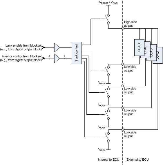
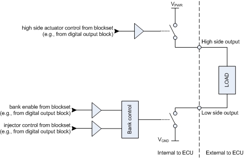
For boosted peak and hold injector outputs, the high-side is switched to regulate current, and the low-side is switched to control recirculation current in the load. The boosted peak and hold injector outputs on one bank must be driven sequentially (may not overlap) and injector outputs on different banks may be driven in parallel (may overlap). When no injector on the bank is active, the high-side and low-side pins are biased to between 3.8V and 5V, this allow for detection of electrical faults on the high-side and low-side pins. Failure to adhere to these requirements may result in malformed injector drive signals.
For non-boosted peak and hold injector outputs, the low-side is switched to regulate current. The non-boosted peak and hold injector outputs can overlap with either with boosted peak and hold injector outputs on the same bank, or with outputs on the other bank.
Each injector must be configured to drive a waveform (as described in Section 4.35, “Digital outputs — waveform control”) before it can be used. The C-API and Sim-API support port and direction injection, including multiple pulses, application based late fuel injection adjustment and ECU based fuel-rail pressure injection adjustment.
Each injector bank must be enabled by setting the output enable pins for the respective bank (e.g. DOT enable). The enable pin can be turned off to quickly disable all injections on a bank if necessary. The enable pin can be overridden with certain hardware configurations and other internal devices. The state of the enable pin can be monitored (e.g. Monitor (enabled)) to check if the pin is overridden or otherwise faulted. The injector outputs are driven from a smart IC with built-in protection from external and internal faults.
The following injector faults are detectable for boosted peak and hold injector outputs:
High-side short-to-battery — A high-side short-to-battery fault will be set for all injectors if no injectors are active when a fault occurs, or a single injector when only that injector is active when the fault occurs. This fault will immediately disable the injector (if active). The fault status will latch and require a rising edge on the reset-fault internal output channel (e.g. DOT reset-fault bank A) before the output can be resumed, even if the fault has gone away.
High-side short-to-ground — A high-side short-to-ground fault will be set for all injectors if no injectors are active when a fault occurs, or a single injector when only that injector is active when the fault occurs. This fault will immediately disable the injector (if active). The fault status will latch and require a rising edge on the reset-fault internal output channel (e.g. DOT reset-fault bank A) before the output can be resumed, even if the fault has gone away.
Low-side short-to-battery — A low-side short-to-battery fault will be set for a single injector only when that injector is active and the fault is detected. This fault will immediately disable the injector. The fault status will latch and require a rising edge on the reset-fault internal output channel (e.g. DOT reset-fault bank A) before the output can be resumed, even if the fault has gone away.
Low-side short-to-ground — A low-side short-to-ground fault will be set for a single injector only when that injector is active and the fault is detected. This fault will immediately disable the injector. The fault status will latch and require a rising edge on the reset-fault internal output channel (e.g. DOT reset-fault bank A) before the output can be resumed, even if the fault has gone away.
Low-side open — A low-side open fault will be set for a single injector only when that injector is inactive and the fault is detected. An open fault cannot be detected while the injector is active. This fault will not disable the injector. The fault status will latch and require a rising edge on the reset-fault internal output channel (e.g. DOT reset-fault bank A) to clear the fault status, even if the fault has gone away.
Boost over-current — A boost over-current fault will be set for a single injector only when that injector is active during a phase where the boost supply has been configured to be driven and the fault occurs. In practice, the boost over-current fault will typically be accompanied by another type of electrical short (e.g. short-to-ground). This fault will immediately disable the injector. The fault status will latch and require a rising edge on the reset-fault internal output channel (e.g. DOT reset-fault bank A) before the output can be resumed.
Note
Because all injectors on a bank share a common high-side pin, and injector loads are typically low resistance, a shorted pin may show up in one or more different injector faults. For example, with no injectors active or open-load, a short-to-battery or ground on the low-side of one injector may also appear as a short on the high-side (through the load), thus disabling all of the injectors on that bank.
The following injector faults are detectable for non-boosted peak and hold injector outputs:
Current-trip — A current-trip fault will be set for a single injector only when that injector is active and the fault occurs. The fault will latch and disable the injector. The current-trip fault can be cleared and the tripped outputs enabled by the pss_OvercurTripReset Simulink block or by calling the pss_overcur_trip_reset() C-API function.
The following injector bank faults are detectable:
Checksum fault (checksum fault) — A checksum fault will be detected if the smart IC has an internal checksum failure. This fault will immediately disable all injectors on the faulted bank. The fault status will latch and require an ECU reset to clear the fault.
Clock fault (clock fault) — A clock fault will be detected if the precision reference clock used by the smart IC has failed. The smart IC will automatically switch to an internal backup clock if this fault occurs. If an injection was active that injection will be aborted and no injections will be possible until after the switch to the backup clock completes. While running on the backup clock, injections are still possible with degraded performance. The fault status can be cleared, by attempting to switch back to the precision reference clock (if not still faulted) by applying a rising edge to the reset clock internal signal. (e.g. DOT reset clock bank A).
Under-voltage VCCP (UVCCP) — A UVCCP fault will be set if smart IC detects an under-voltage on the internal 7V power supply. This fault will immediately disable all injectors on the faulted bank. If the fault condition clears the smart IC will automatically recover.
Under-voltage VCC5 (UVCC5) — a UVCC5 fault will be set if smart IC detects an under-voltage on the internal 5V power supply. This fault will immediately disable all injectors on the faulted bank. If the fault condition clears the smart IC will automatically recover.
Over-temperature (ot) — An over-temperature fault will be set if smart IC detects an internal temperature greater than 177°C nominal. This fault will not disable any injectors. If the fault condition clears the fault status also will clear.
Self test run (self-test run) — At ECU initialization, the Built-In-Self-Test (BIST) of the smart IC is run. This may take a few hundred milliseconds to complete. Once the test is complete, this signal will be set. All injectors will be disabled while this signal is low.
Self test pass (self-test pass) — At ECU initialization, the Built-In-Self-Test (BIST) of the smart IC is run. This may take a few hundred milliseconds to complete. If the (self-test run) signal is set, the (self-test pass) signal indicates the results of the BIST. If set high, the BIST successfully passed, if set low, the BIST has failed. If the BIST has failed, all injectors will be disabled. An ECU reset will be required to clear the fault.
Current-trip — A current-trip fault will be set for all injector bank high sides when any injector is active during a phase where the battery supply has been configured to be driven and the fault occurs on the high side output. The fault will latch and disable all injector banks The current-trip fault can be cleared and the tripped outputs enabled by the pss_OvercurTripReset Simulink block or by calling the pss_overcur_trip_reset() C-API function.
There are a several monitor signals which can be used for diagnostics purposes for the boost power supply used for injections. The boost supply has an internal voltage monitor (see AIN boost-voltage). A large drop in voltage can indicate that the injectors are drawing too much power from the supply. This can be due to several combining factors, which depends on the duration that the boost supply is on during each injection, the current limit during the boost phase, and the total frequency of injections across all injectors. There is also an over-voltage monitor for the boost supply (see Monitor (ov)). If the boost voltage is greater than 65V this flag will be set and the boost supply will automatically turn off, until the voltage falls back below the threshold.
There are also two duration diagnostic measurements useful to determine if the boost supply cannot maintain the voltage threshold. The Monitor (max recharge time) time is a measure of maximum time it took to recharge the boost supply since last read. A large value could indicate that it took longer than normal to restore the boost supply voltage level. The Monitor (recharge time) time is a measure of the instantaneous recharge time. If the boost supply cannot recharge back to the voltage set-point it will continue to attempt to recharge, and this value will continue to increase until it saturates at 6.5535 seconds. This would indicate a failure in the boost supply.
The non-boosted peak and hold injector outputs have analogue voltage monitors which can be used for diagnostic purposes. (e.g. Monitor (v)) to detect electrical shorts while the outputs are not actively driven.
The M670N ECU has been modified to drive overlapping non-boosted peak and hold solenoid injectors. Unlike the M670B module, the M670N module can overlap injectors on the same bank in addition to injectors on different banks. The ECU does not have a boost power supply, and thus the high-side output pins (bank A Z1 and bank B Z5) will drive only battery (VPWR) to the load when active.
The low-side output pins Y18 and Y53 remain the same on the M670N as on the M670B. The low-side output pins Z6 and Z17 are disabled on the M670N. The low-side output pins Z18, Z30 and Z42 on bank A and Z29, Z41 and Z53 on bank B have been modified as overlapping non-boosted peak and hold injector outputs. Thus the available low-side output pins on the M670N ECU are Y18, Z18, Z30 and Z42 for bank A and Y53, Z29, Z41 and Z53 for bank B.
All boosted peak and hold injector faults and injector bank faults from Section 4.38, “Digital outputs — injection driver protection”, except for the Boost over-current fault, also apply to the M670N ECU. The Y18 and Y53 pins have overcurrent trips, but the remaining pins (bank A Z18, Z30 and Z42 and bank B Z29, Z41 and Z53) do not have overcurrent trips. The overvoltage, max recharge time, and recharge time monitors from Section 4.39, “Digital outputs — injection monitors” do not apply to the M670N ECU. The boost supply internal voltage monitor will continue to function, but will return battery voltage.
The M670N module still requires waveform configuration as described in Section 4.35, “Digital outputs — waveform control” but will ignore any boost voltage settings. Any waveform configured to drive boost voltage during a phase will drive battery voltage instead. The boost voltage setpoint will be ignored.
The M670S ECU has been modified to drive overlapping saturating solenoid injectors. Unlike the M670B module, the M670S module can overlap injectors on the same bank in addition to injectors on different banks. The ECU does not have a boost power supply, and thus the high-side output pins (bank A Z1 and bank B Z5) will drive only battery (VPWR) to the load when active. The same low-side output pins for each bank as the M670B are used (bank A Z6, Z18, Z30 and Z42 and bank B Z17, Z29, Z41 and Z53).
Each injector bank must be configured the same as the M670B, as displayed in the Figure 4.22, “Injector boosted peak and hold bank diagram” diagram, except that the high side can only supply (VPWR).
The high-side is shared between all low-sides on a bank. On the M670S ECU, the high-side is turned on when at least one injector is active, and stays on until all injectors on the bank are inactive. When all injectors on a bank are inactive, the bias voltage should be present on all pins. The high-side and low-side are both turned on at the same time, but neither are PWM'd to regulate current when an injector is active. The four injectors on a bank are grouped into two pairs which share a common current sense. On bank A, injectors Z6+Z18 share a current sense, and injectors Z30+Z42 share the other current sense. On bank B, injectors Z17+Z29 share a current sense, and injectors Z41+Z53 share the other current sense. If the combined current through each pair of injectors exceeds 6A, both outputs will be latched off (see the internal Current-trip monitors bank A Monitor (ct) and Monitor (ct); bank B Monitor (ct) and Monitor (ct)) These current trips can be cleared with a rising edge on the reset-fault internal output channel (e.g. DOT reset-fault bank A).
The M670S module will ignore any configured waveforms as described in Section 4.35, “Digital outputs — waveform control” for the saturating injectors.
All boosted peak and hold injector faults and injector bank faults from Section 4.38, “Digital outputs — injection driver protection”, except for the Boost over-current fault, also apply to the M670S ECU. The overvoltage, max recharge time, and recharge time monitors from Section 4.39, “Digital outputs — injection monitors” do not apply to the M670S ECU. The boost supply internal voltage monitor will continue to function, but will return battery voltage.
The non-boosted peak and hold outputs, remain the same as the M670B ECU (bank A Y18 and bank B Y53) and can be configured as described in Section 4.35, “Digital outputs — waveform control”.
The digital outputs related to smart ignition coils (pins Y37, Y38, Y39, Y40, Y44, Y45, Y49 and Y50) are logic signals used to activate the smart coils. In the standard M670 build, these outputs provide an internal pull-up to VREFD XG2.
The digital outputs related to smark ignition coils have the following protection features:
Over-voltage clamp protection — The potential on the output pin is clamped to a maximum voltage, of between 40V and 55V (typically 45V).
Over-temperature protection — The output is cut off when the temperature detected by the protection circuitry exceeds a threshold. The threshold lies between 150°C and 200°C, with a typical value of 175°C. The output is re-enabled when the temperature falls to about 15°C below the cut-off temperature. The temperature cut-off applies to the pairs of outputs that share the same protection circuitry. The outputs are paired as follows: Y37 and Y38, Y39 and Y40, Y44 and Y45, and finally, Y49 and Y50. Over-temperature protection provides effective protection against short circuit.
Current limiting — Individual outputs are rated to 360mA for non-transient operation. Transient currents are limited to a maximum current of between 1.7A and 3.5A. This maximum current applies to the total current on the pairs of outputs listed above. In practice, over-current will rapidly lead to an over-temperature condition being detected, causing the paired outputs to turn off.
Each of the ignition outputs has a corresponding synchronous digital monitor. The ECU samples the state of the digital monitor (with a delay) each time the requested output state changes. If the reported output state differs from the requested output state, the corresponding synchronous digital monitor counter (one for falling edge, one for rising edge) is incremented. The application can read the counters to determine whether an electrical fault exists.
For a falling edge, i.e. when the output is activated, the time threshold is 230 us. If the monitor feedback signal still reads high this long after the output was activated, then the output is disabled by the platform software, and must be re-enabled by the application. (Independently, the output device itself will respond to over-temperature as described in the previous section.)
For a rising edge, i.e. when the output is deactivated, the time threshold must be set by the application. Table 4.11, “Recommended rise-time thresholds with load” provides advice for setting the time threshold. The values in this table assume purely resistive loads pulled up to 5V. Pulling up to battery will reduce the rise-times a little. The ideal time threshold can be characterized on each system using an oscilloscope. No intervention is made by the platform software in the case when the monitor feedback failed to read high after this time.
Table 4.11. Recommended rise-time thresholds with load
| Load | Threshold |
|---|---|
| 100 Ohms | 250 us |
| 1K Ohms | 400 us |
| 5K Ohms | 1200 us |
Note
These recommended thresholds are currently under review and may be amended in future versions of this document.
The potentials on the output pin corresponding to guaranteed low and guaranteed high are 2.1 and 4.0 V respectively. The actual thresholds will lie somewhere in between, and will depend on operating conditions.
Some digital outputs (pins XB1, XG2, XH2+Z14, XJ2+Z8, XK2+Y8, XL1, XL3, XL4+XM4, XM1, XM2+XM3, Y1, Y5, Y6, Y18, Y28, Y29, Y30+Y42, Y37, Y38, Y39, Y40, Y41, Y44, Y45, Y49, Y50, Y53, Z31, Z36, Z37, Z38, Z39 and Z43) can be monitored for over-current events. The over-current trip state of an output pin is monitored using a corresponding internal over-current monitor channel. In normal operation the internal over-current trip channel will be one. If the output channel experiences an over-current, the output channel will be forced off by the ECU and the over-current trip channel will be set to zero.
Once an over-current trip occurs, the recommended procedure is to clear the trip and resume normal operation. If the fault condition is confirmed by another trip, then the recommended action is to disable the output for the remainder of the ignition cycle.
Repeatedly re-enabling an output driver that has automatically shut off can shorten the lifetime of that output circuit. This is particularly true for devices with built-in thermal protection, which shut off well above their rated maximum temperatures in order to accommodate the tolerances required to operate at their rated maximum temperatures. Once shut off, these require time to cool down, even after they are thermally re-enabled, so that total time of temperature excursions is limited to a small number of hours during the life of the ECU.
The over-current trip latch can be cleared and the tripped outputs enabled by the pss_OvercurTripReset Simulink block or by calling the pss_overcur_trip_reset() C-API function.
Note
To help component heat dissipation and to help prevent component stress, the platform software ensures there is at least 50ms between each request to clear the over-current trip latches.
The H-bridge outputs (pins XL4+XM4, XM2+XM3 and Y30+Y42 in the standard build, and pins XB4+XC4, XE2+XF2, XE4+XF4 and XJ4+XK4 if the H-bridge and SENT daughterboard is fitted) are controlled through the pdx_HBridge_Output Simulink block or the pdx_hbridge_output() C-API function. The outputs are capable of driving actuators of 10 mH up to 500 Hz PWM, of 1 mH between 500 Hz to 5 kHz, and of 500 uH between 5 kHz and 10 kHz.
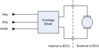
The H-Bridge can be driven in four modes:
- No Drive
In no-drive mode, the H-bridge is turned off leaving the pins to float.
- Brake
In brake mode, both pins of the H-bridge are driven to VPWR.
- Forward
In forward mode, pin XM4, XM2, Y30, XC4, XF2, XF4, or XK4 is driven to VPWR and pin XL4, XM3, Y42, XB4, XE2, XE4, or XJ4 pulsed to VGND, resulting in a current flow the opposite from the reverse mode.
- Reverse
In reverse mode, pin XL4, XM3, Y42, XB4, XE2, XE4, or XJ4 is driven to VPWR and pin XM4, XM2, Y30, XC4, XF2, XF4, or XK4 is pulsed to VGND, resulting in a current flow the opposite from the forward mode.
Warning
To avoid unexpected behavior, H-bridges should be set to NO DRIVE mode before flashing the ECU. This can be done by commanding the actuators to NO DRIVE any time the engine is not turning.
The frequency and the duty cycle of operation are controlled by the application. Voltage and current monitors are available, see Section 4.48, “H-bridge outputs — monitors” for details.
In order to ensure accurate over-current protection on some H-bridge outputs (pins XL4, XM4, Y30 and Y42), certain PWM frequency bands are not allowed by the platform. If the application software sets the PWM frequency to be within one of the disallowed frequency bands, the platform will automatically select the closest allowed frequency. The disallowed frequencies are given in the following table.
Table 4.12. H-bridge disallowed frequencies
| Low (Hz) | High (Hz) |
|---|---|
| 6253.50 | 6293.50 |
| 3126.75 | 3146.75 |
| 1563.37 | 1573.38 |
| 781.688 | 786.688 |
| 390.844 | 393.344 |
| 195.422 | 196.672 |
| 97.7109 | 98.3359 |
| 48.8555 | 49.1680 |
| 24.4277 | 24.5840 |
| 12.2139 | 12.2920 |
| 6.1069 | 6.1460 |
| 3.0535 | 3.0730 |
| 1.5267 | 1.5365 |
| 0.7634 | 0.7682 |
Some H-bridge outputs (pins XL4, XM4, Y30 and Y42) can be controlled as individual half-bridge, high-side or low-side outputs. For each of these pins, there is a corresponding internal control signal that can be used to control the mode (for instance, XL4 and DOT select-hs).
- Half-bridge mode
To drive the pin as a half-bridge, set the digital output to 1 and drive the internal select-hs digital output as a PWM. This will cause the output pin to PWM between VGND and VPWR.
- High-side mode
To drive the pin as a high-side driver, set the internal select-hs digital output to 1 and drive the digital as a PWM. This will cause the output pin to PWM between VPWR and open.
- Low-side mode
to drive the pin as a low-side driver, set the internal select-hs digital output to 0 and drive the digital as a PWM. This will cause the output pin to PWM between VGND and open.
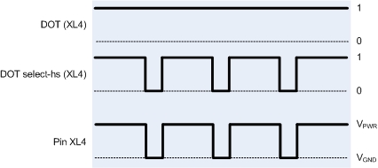
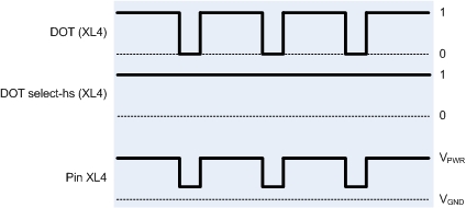
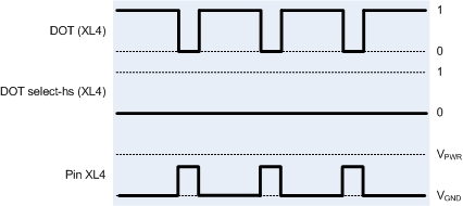
Note
The controlling digital output channels can both be driven as PWM outputs at the same time. It is recommended that for determinate behaviour only one of the controlling digital outputs is driven as a PWM at a time.
Warning
If the ECU is being used in a mixed-voltage system where the external high-side voltage of the load is different from the high-side voltage of the ECU, then it is recommended that the half-bridge pin not be used.
All of the H-bridge output pins XL4, XM2, XM3, XM4, Y30 and Y42 (including pins XB4, XC4, XE2, XE4, XF2, XF4, XJ4 and XK4 if the H-bridge and SENT daughterboard is fitted) provide voltage monitors. The voltage readings are not synchronised with the on stage of the PWM drive signal, so care must be taken when using the voltage monitor to diagnose electrical faults.
When the H-bridge is in no-drive mode, the outputs will float at the bias voltage such that the voltage monitors read approximately 0.41V to 0.53V. This can be used to diagnose short-to-ground and short-to-battery faults, when the pin reads 0V or battery voltage respectively. Open-load faults can be detected by driving just one arm of the H-bridge either high or low and checking if the other arm remains at the bias voltage.
A subset of the H-bridge output pins XL4, XM4, Y30 and Y42 (including pins XB4, XC4, XE2, XE4, XF2, XF4, XJ4 and XK4 if the H-bridge and SENT daughterboard is fitted) provide current monitors. These analogue inputs provide a current reading when the corresponding output is fully switched to the high-side. Thus, when operating the H-bridge with a PWM low-side, the application must read the current measurement from the monitor on the high-side pin. If the H-bridge switches direction, the application should switch to reading the current from the other pin.
The current reading when the corresponding output is fully switched to the low-side, is the driver device current offset, IS. The value is approximately 0.2V, hence the equation given with the current monitors. A more accurate current reading can be achieved by substituting IS for the value 0.2.
The current monitors on the output pins XL4, XM4, Y30 and Y42 also function as over-current fault flags. When the current monitor input reads above 3.96V, this indicates that the device has gone into fault mode and shut off. The H-bridge will need to be set to no-drive mode to reset the device and return to normal operation.
The remaining H-bridge (pins XM2+XM3) provides a fault monitor flag on channel Monitor (no fault). If an over-current fault occurs, the signal will be set to low indicating the device has gone into fault mode. The H-bridge will need to be set to no-drive mode to reset the device and return to normal operation.
An exhaust oxygen sensor measures the remaining oxygen content in the exhaust gas so the engine can determine the amount of fuel required to ensure optimal emissions. The M670 provides the capability to sense narrow and wide band oxygen sensors.
The M670 supports narrow band EGO sensors (often referred to as HEGO sensors, for Heated Exhaust Gas Oxygen, or two step lambda oxygen sensors) on pins XJ1 and XK1. A HEGO sensor generates an indication of whether the exhaust gas mixture is lean or rich. The sensor should return a voltage between 50mV and 900mV, centered around the stoichiometry control point, typically 425mV. Generally the sensor will return 50mV to 300mV in the Lean or higher air content condition, and will return between 600mV and 900mV in the Rich or higher fuel content. Refer to your HEGO sensor data sheet as each sensor may be different.
To control the HEGO sensor's internal heater, any of the higher current low-side driver outputs can be used (pins XL1, XM1, Y6, Y18, Y29, Y41 and Y53). Unlike the UEGO sensors, which require certain low-side driver outputs to be used, there is no restriction for HEGO sensors.
As a build option, a M670 ECU can be ordered with four HEGO inputs and zero UEGO inputs.
The M670 supports two wide band EGO sensors (often referred to as UEGO sensors, for Universal Exhaust Gas Oxygen, or linear lambda oxygen sensor) on pins Z10, Z11, Z22 and Z23 and Z34, Z35, Z46 and Z47. A UEGO sensor generates an indication of the oxygen content in the exhaust gas mixture. UEGO sensors require careful control of the resistive heating element to avoid damaging the ceramic heater, and careful control of the pump cell current to accurately measure the oxygen content.
The ECU provides UEGO inputs processed by Bosch CJ125 ASICs.
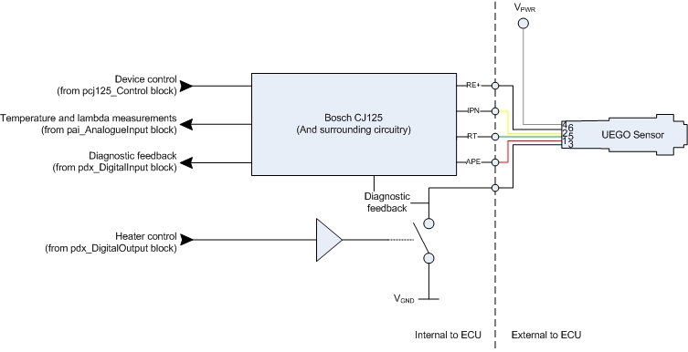
The CJ125 ASICs are controlled through the pcj125_Control Simulink block or the pcj125_control() C-API function. This interface gives the application direct control over the ASIC's internal configuration. The actual control algorithm will need to be defined by the application. See the OpenECU User Guide for more details.
To control the UEGO sensor's internal heater, each CJ125 device has a corresponding low-side driver output (pins Y29 and Y41). These outputs are controlled as standard low-side drivers (see Section 4.27, “Digital outputs” for more) but have internal connections to their corresponding CJ125 devices, to provide diagnostic information to the ASIC.
Note
M670 comes standard with support for the Bosch LSU 4.9 UEGO sensor. If you would like to use a different UEGO sensor, Contact Pi for further information.
Note
It is recommended that the Bosch LSU 4.9 Heater+ (pin 3) is connected to one of the actuator supplies (pins Y1 and Y5) rather than directly to VPWR to allow the heater to be shut off if a short-circuit fault occurs.
Warning
The application must actively manage the sensor's resistive heater control in order to ensure the sensor ceramic is not damaged. The Bosch LSU 4.9 sensor can be used in a 24V system, but the application must actively manage the heater control such that the heater never sees more than 12V for longer than 20 seconds or damage can occur. It is recommended that the low-side driver for pins Y29 and Y41 are never run at 100% duty cycle.
When the Bosch LSU 4.9 sensor is used with a power source greater than 20V, especially when the sensor is cold, the sensor's heater resistance can be as low as 1.3 Ohms. The resulting current flow for any significant drive duty cycle can exceed the over-current trip thresholds for pins Y29 and Y41. In turn, the ECU will attempt to protect itself and the sensor by turning off pins Y29 and Y41 and signalling an over-current event. To avoid this:
Use a low-duty, high-frequency drive signal to avoid the output reaching the over-current trip threshold. This is especially relevant when the sensor is below ambient temperature. During the condensation water phase of the sensor warm-up, the LSU 4.9 datasheet suggests an effective RMS of 1.5V, which must be matched by the drive signal to ensure the over-current trip threshold is never met.
Use a lower voltage source to power the sensor. In this situation, the ECU will accomodate a mixed voltage system, where the ECU is powered at 24V and the sensor as 12V (for example).
Use a higher-current low-side drive pin for the heater control, such as pin Y6 or Y30. When not using pins Y29 and Y41 for heater control then note that the electrical diagnostic signals from the CJ125 ASIC (Monitor (ol), Monitor (sb) and Monitor (sg) for pin Y29, and Monitor (ol), Monitor (sb) and Monitor (sg) for pin Y41) are inoperative and should be replaced by relevant monitors for the chosen drive pin.
Note that if the ECU is being used in a 24V system, then short-to-battery faults and voltages above 28V can damage the CJ125 device. The CJ125 device supports up to 18V.
See the Bosch sensor data sheets, or contact Bosch, for further information.
To read the UEGO sensor's temperature for closed-loop control, each CJ125 device provides a measurement of the UEGO heater's resistance via a UR analogue input channel. The correct transfer function will need to be used to convert this to engineering units.
To read the UEGO sensor's lambda value, once the device provides a valid value, each CJ125 device provides a UA analogue input channel. The application is responsible for making the calculations to determine the actual lambda value.
The Bosch CJ125 devices (pins Z10+Z11+Z22+Z23 and Z34+Z35+Z46+Z47) provide serial diagnostic information which the platform automatically decodes into digital input channels. The diagnostic information is sampled at the fastest task rate of which one of the corresponding diagnostic inputs is read (see Section 4.33, “Digital outputs — monitors (conditioned)” for further details).
The open-load monitors (channels Monitor (ol) and Monitor (ol)) indicate if the heater pin is disconnected from the heater load.
The short-to-ground monitors (channels Monitor (sg), Monitor (sg), Monitor (sg), Monitor (sg), Monitor (sg), Monitor (sg), Monitor (sg) and Monitor (sg)) indicate if the voltage on the corresponding UEGO-related pin is at a voltage too close to VGND.
The short-to-battery monitors (channels Monitor (sb), Monitor (sb), Monitor (sb), Monitor (sb), Monitor (sb), Monitor (sb), Monitor (sb) and Monitor (sb)) indicate if the voltage on the corresponding UEGO-related pin is at a voltage too close to VPWR.
The ECU provides for secondary processor for monitoring and safety purposes as a build option (the default build does not have the secondary processor populated). The secondary processor uses an independent clock source, has access to a subset of the input signals, can communicate with the primary processor and can inhibit the injector circuitry independently from the primary processor.
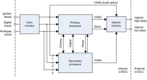
Table 4.14. Secondary processor connector pin access
| Channel | Type | Description |
|---|---|---|
| Y25 | Digital input | Allows the secondary processor to inhibit the injector circuitry if the operator requests shut down through the ignition sensor pin. Note that there is a build option to inhibit the injector circuitry directly from the ignition sense input. |
| Z12 | Digital input | Access to one of two switched digital inputs, such as the low oil switch. |
| Z13 | Digital input | Access to one of two switched digital inputs, such as the brake switch. |
|
Z20
Z21 | Analogue input | Access to two throttle position inputs for the purposes of cross checking with the primary processor. |
|
Z27
Z28 | Analogue input | Access to two pedal position inputs for the purposes of cross checking with the primary processor. |
As well as access to a small subset of connector pins, the secondary processor has access to a small subset of the ECU's internal signals.
Table 4.15. Secondary processor internal signal access
| Channel | Type | Description |
|---|---|---|
| AIN +2.5V | Analogue input | Access to the precision 2.5V reference for ratiometric conversion of other analogue inputs (if required). |
|
Monitor (v)
Monitor (v) | Analogue input | Access to the voltage monitors for VREFA and VREFB, both for ratiometric conversion of other analogue inputs (if required) and to monitor the sensor supply for faults when performing cross checking. |
| AIN PCB-temp | Analogue input | Access to the internal temperature of the ECU, used for cross checking. |
| AIN VPWR | Analogue input | Access to the ECU's power supply voltage, used for cross checking. |
|
DIN pri-sec-a
DIN pri-sec-b DOT pri-sec-a DOT pri-sec-b | Digital | Access to two digital lines, which can be setup as digital inputs or outputs as agreed between the applications running on the primary and secondary processors. Used for signaling between the processors. |
| DOT inhibit (pin Y18, Y53, Z1, Z5, Z6, Z17, Z18, Z29, Z30, Z41, Z42, Z53) | Digital output | Access to inhibit the injector circuitry, including the boost supply (if available) and injector related outputs. |
| DOT reset-primary | Digital output | Access to reset the primary processor from the secondary processor. The primary processor can similarly reset the secondary processor. |
| Serial | Communications | Bi-directional communications between the secondary and primary processor. Used by the primary processor for reprogramming whilst the ECU is in reprogramming mode. Used by the secondary processor whilst the ECU is in application mode to exchange questions and answers during cross checking. |
This option is not yet supported. Contact Pi for further information.
The ECU has been designed to be able apply the E-Gas monitoring concept guidelines as detailed in “Standardized E-Gas Monitoring Concept for Gasoline and Diesel Engine Control Units”, v5.5 May 2013. The E-Gas monitoring concept breaks the functionality of the ECU into three distinct levels across two independent devices.
- Level 1 — function
Contains the engine control functions (for instance, requested torque, component monitoring (for instance, correlated pedal position or a faulted lambda sensor), input/output variable diagnostics (such as requests for additional torque from other ECUs), and the reaction to detected faults.
- Level 2 — function monitoring
Contains the diagnostic functions for level 1 engine control (for instance, measuring injection pulses to estimate torque and cross check with level 1 requested torque or vehicle acceleration) and program flow monitoring (for instance, that software tasks run in sequence and to deadlines), and the reaction to detected faults.
- Level 3 — controller monitoring
Contains the diagnostic functions for level 1 and level 2 software interactions with hardware (for instance, cyclic testing of RAM cell content for bit inversions, or processor instruction testing).
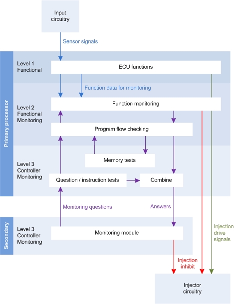
Level 3 is further split into two parts:
- Level 3 — monitoring module
Physically independent monitoring device (secondary processor on the M670) that communicates a series of questions to determine if the function device (primary processor on the M670) is acting as it should. The answer to each question is checked for timeliness and correctness, provoking a reaction if unexpected.
- Level 3 — monitoring software
Contains the software to combine the results of level 2 and level 3 responses to the questions from the level 3 monitoring module.
Software support for the secondary processor and to allow implementation of the E-Gas monitoring concept are not yet available. Contact Pi for further information.
Some of the internal and external inputs and outputs are classed as serial. The connector pinout tables and internal channel tables above specify whether a pin or channel is serial or not.
When a serial input is read, the measurement reflects the value of the input taken last time the application task ended. I.e., the value of the input is delayed by one cycle of the task period. When a serial output is set, the driven state is updated at the end of the current application task. I.e., there is a delay between requesting a change in the output state, and the output state honoring that request.
The CAN buses (pins Y12+Y11, Y24+Y23, Y36+Y35 and Y48+Y47) are implemented using high-speed CAN transceivers, compatible with J1939. Only the default CAN bus (pins Y12+Y11) has a terminating resistor fitted; the other CAN buses require external termination.
Some CAN buses (pins Y11, Y12, Y23 and Y24) have wake-on-CAN functionality (see Section 4.4, “ECU power — wake-on-CAN” for more details).
The M670 is designed to support LIN communications. However, this option is not yet supported. Contact Pi for further information.
The M670 is designed to support FlexRay communications. However, this option is not yet supported. Contact Pi for further information.
The ECU supports different memory configurations for application, calibration and RAM sizes, some of which require a TAB board (see Section 4.62, “Memory — calibration capabilities”).
Table 4.16. Memory configurations supported
|
Configuration |
App size (KiB) |
Cal size (KiB) |
RAM size (KiB) |
External RAM required? |
Run-time
calibration supported? |
|---|---|---|---|---|---|
| A [a] | 3072 | 128 | 128 | N | Y |
| B | 3072 | 64 | 192 | N | Y |
| C | 3072 | 192 | 64 | N | Y |
| D | 3072 | 512 | 256 | N | N |
| 3072 | 512 | 256 | Y | Y | |
[a] If an OpenECU target that supports memory configuration is loaded with an application in which no such configuration has been specified, then configuration A will be used as the default. | |||||
The ECU supports non-volatile memory storage in Flash. Battery backed RAM is not supported.
The processor's Flash memory is split into small and large memory blocks. The application and calibration are stored in large blocks, whilst DTC information, freeze frames and so on are stored in small blocks.
The largest Flash block can take up to approximately 15 seconds to erase. This occurs in an environment where the Flash has been erased and programmed many times at its temperature extreme. The typical erase time is smaller, especially at ambient temperatures. Reprogramming an ECU (where many large blocks would be erased), or storing DTC information across power cycles, can therefore take some time. Users and applications should take this into consideration.
The minimum number of erase cycles is approximately 1,000 for large Flash blocks and 100,000 for small Flash blocks. This occurs in an environment where the Flash has been erased and programmed many times at its temperature extreme. The typical number of erase cycles is larger, especially at ambient temperatures.
The minimum data retention is approximately 5 years for blocks which have been erased less than 100,000 times, and approximately 20 years for blocks which have been erased less than 1,000 times.
The information about the Flash has been taken from Freescale's MPC5674F Microcontroller Data Sheet document, revision 9 (dated Nov 2012).
The ECU has the capability to accept calibration changes while the application software is running. There are two types of calibration options accessible via the memory configuration selection in software:
Primary processor's RAM — Dedicates some of the processor's RAM for calibration purposes. This option reduces the amount of RAM available for the application and supporting platform library. This option is available on a standard build of the ECU and is the default if the application does not specify a memory configuration.
TAB board RAM — Uses a daughter board to add a RAM device to the memory bus of the primary processor. This option provides all of the processor's RAM for the application and platform library, whilst adding additional RAM to support calibration. This option is available as a build option.
The design of the ECU includes support for VertiCal based memory interfaces, such as ETAS's XETK. These devices provide high speed data logging and calibration, an order of magnitude better than CCP. Contact Pi for further information.
The ECU can run in one of two system modes: reprogramming mode and application mode. In reprogramming mode, both processors of the ECU can be reprogrammed with application software from a calibration tool. In application mode, the ECU runs the programmed application software.
The ECU enters reprogramming mode either by measuring a dedicated external pin called FEPS (pin Y22) at power up, or when attempting to reflash over CCP when the application is not inhibiting reprogramming.
Table 4.17. System mode selection
| Voltage | System mode |
|---|---|
| > +17V | Enter reprogramming mode. If valid application software has previously been programmed, then use the CCP settings from that application, otherwise use the default CCP settings. |
| < -16V | Enter reprogramming mode. Use the default CCP settings. |
| Otherwise | Enter application mode if valid application software has previously been programmed, otherwise enter reprogramming mode. |
The ECU has a dedicated external pin (pin Y28) for flashing a lamp.
The flash sequence represents a set of codes. Each code is a three digit number, where each digit is flashed a number of times equal to its value. An example would be the flash sequence for code 113. The flash sequence is broken down into a series of marks, or on and off pulses as follows:
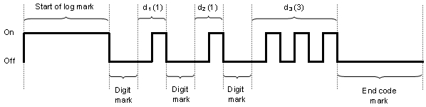
Each of the marks lasts for a specific duration:
Table 4.18. Flash code example
| Mark | Duration and meaning |
|---|---|
| Start of log mark | 3s — marks the start of the flash code list |
| Digit mark | 1s — marks the start of a digit |
| dn | ns — n digits, where the output is turned OFF for 0.5 second, then ON for 0.5 seconds, n times |
| End code mark | 3s — marks the end of a code (i.e., end of 3 digits) |
After the end code mark, the ECU will either flash the next code, or return to the start of the list and flash the first code. The ECU always has at least one code to flash.
Each code represents information about the ECU state. If there is no flash sequence, or a malformed flash sequence, then the ECU is malfunctioning. Otherwise, the flash sequence will represent one of the following codes:
Table 4.19. Flash codes
| Code | Meaning |
|---|---|
| 111 | In application mode — no other condition has been detected. |
| 112 | In reprogramming mode with the FEPS pin negative. |
| 113 | In reprogramming mode with the FEPS pin high. |
| 114 | In reprogramming mode via a FEPS-less reprogramming request. |
| 115 | In reprogramming mode because no valid application software exists. |
| 116 | In reprogramming mode due to FEPS pin electrical failure. |
| 117 | In reprogramming mode due to repeated reset during application mode. |
| 118 | In reprogramming mode due to failed application checksum tests. |
| 128 | In reprogramming mode due to failed memory check tests. |
| 119 | In reprogramming mode due to a FEPS-less ISO reprogramming request. |
| 121 | In reprogramming mode due to an unknown failure. |
| 123 | In reprogramming mode due to a watchdog reset. |
| 222 | In reprogramming mode due to the application not having a valid license. |
The ECU closely adheres to the IEEE-754 for floating point numbers.
When using Simulink, floating point Simulink models are supported — all calculations are performed using single-precision (even if the model uses double-precision, the ECU performs calculations using single-precision).
When using the C-API, floating point applications are supported — all calculations are performed using single or double precision, as determined by the application code (although double precision will incur some software overhead — see the compiler reference manual for further details).
The rounding mode is set to round-to-nearest. In some conditions, the ECU will not adhere to the IEEE-754 standard:
Table 4.20. Floating point conditions
| Condition | Result |
|---|---|
| Underflow | The result of a calculation underflow is ±0. The sign is based on the signs of the operands. |
| Overflow | The result of a calculation overflow is ±max where max is approximately 3.4 × 1038. The sign is based on the signs of the operands. |
| Divide by zero |
The ECU does not generate ±Inf, NaN or a denormalised number as the result of a calculation.
Simplified schematics of the input and output circuitry will be made available in a subsequent release.
To support a variety of sensors and actuators, the ECU is pre-populated with a default selection of components with varying voltage range, pull strengths, filtering and other characteristics. In some cases, the default component selection will not meet the requirements of all customers. Within design constraints, Pi can modify the ECU components to adjust these characteristics as build options. Contact Pi for further information.
The ECU has been designed for easy configuration by the addition of a plug-in daughter board. The main circuit board can be configured to route a range of internal processor signals and external connector pins, XA1, XA2, XA3, XA4, XB4, XC4, XE2, XE4, XF2, XF4, XJ4 and XK4, to the plug-in location of the daughter card. Within design constraints, Pi can develop prototype quality daughter board to implement a wide range of functions. Contact Pi for further information.
The following sections outline the daughterboards which affect channel selection. Other daughterboards may be available.
The daughterboard extends the available H-bridges to pins XB4+XC4, XE2+XF2, XE4+XF4 and XJ4+XK4, and adds support for SENT sensors on pins XA1, XA2, XA3, XA4 and XF3 based on SAE J2716 Revision 2010. To use the additional H-bridge channels, see Section 4.46, “H-bridge outputs”. To use the SENT channels, see the C-API or Sim-API User Guide for further details.
The daughtercard utilises unused channels on the PCB as well as repurposing existing channels. Repurposed channels are non-functional when the daughtercard is fitted.
- LIN and FlexRay communication support is unavailable with the daughterboard.
- The digital input for pin XF3 is unavailable with the daughterboard.
- The digital monitor for injector channels Z42, Z17 and Z29 is unavailable with the daughterboard.
- The digital monitor for smart spark channels Y44, Y45, Y49 and Y50 is unavailable with the daughterboard.
The ECU has the following mechanical dimensions (mm):
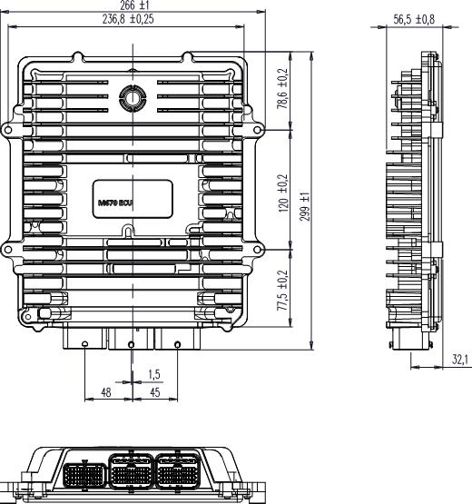
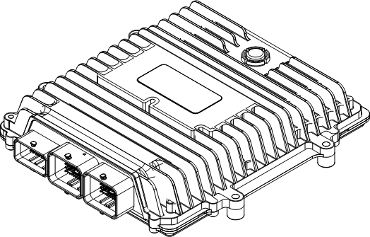
If you have questions, or are experiencing issues with OpenECU please see the FAQ website:
- website
If you still have questions after searching through the FAQ, or want to discuss sales or proposals, you can contact main office:
- Tel
- +1 734 656 0140
- Fax
- +1 734 656 0141
during normal working hours (Mon to Fri, 0930 to 1700 EST).