Release 2.9.0 (r2020-1)
Copyright © 2020 Pi Innovo
13-Apr-2020
Table of Contents
- 1. Technical specification
- 2. Connector pinout
- 3. Internal signals
- 4. Operational details
- 4.1. ECU power
- 4.2. ECU power — control
- 4.3. ECU power — sensor supplies
- 4.4. Analogue inputs
- 4.5. Analogue inputs — ratiometric measurement
- 4.6. Analogue inputs — internal temperature input
- 4.7. Analogue inputs — relationship between VREF, sensor supplies and inputs
- 4.8. Digital inputs
- 4.9. Digital outputs
- 4.10. Digital output — state monitoring
- 4.11. Digital output — low-side driver protection and diagnostics
- 4.12. Injector outputs — operation
- 4.13. Injector outputs — open circuit and short-to-ground diagnostics
- 4.14. Injector outputs — short-to-battery diagnostics
- 4.15. Variable resistance output — operation
- 4.16. Variable resistance output — over current protection
- 4.17. CAN communication busses
- 4.18. Memory — non-volatile storage and lifetime
- 4.19. System modes
- 4.20. Floating point capabilities
- 5. Dimensions
- A. Contact information
List of Figures
List of Tables
- 1.1. Specification
- 1.2. Function reference
- 2.1. Part numbers of the mating connector
- 2.2. Part numbers for the 6.3 mm pin
- 2.3. Part numbers for the 2.8 mm pin
- 2.4. Part numbers for the 0.64 mm pin
- 2.5. Part numbers of the pin crimp tools
- 2.6. Connector pinout — Pocket A
- 3.1. Internal signals
- 4.1. PSU 1 monitor voltages
- 4.2. Digital input thresholds
- 4.3. Injector trigger input thresholds
- 4.4. Low-side digital output leakage current
- 4.5. Low-side digital output thermal trip
- 4.6. Injector current thresholds
- 4.7. Injector Diagnostic Monitor(v) thresholds
- 4.8. Injector Diagnostic Monitor(sb) levels
- 4.9. System mode selection
- 4.10. Floating point conditions
This document is the technical specification for OpenECU part 01T-068696-000 Issue 1. Within this document, that part is referred to as the M221-000 ECU.
Note
For a list of issues and possible work arounds for this ECU, found after publication of this document, please refer to the hardware errata for this ECU (named 29T-068696 M221 Technical Spec Errata).
Specific option control may exist for this part. In that case, parts of this document will be overridden by an option control specific technical specification. Please refer to the option control technical specification for more information.
This technical specification relates to the following ECU variant:
M221D-000 — for development and testing, including full interactive calibration tool integration.
Table 1.1. Specification
| Specification | Variant |
|---|---|
| M221D-000 | |
| Status | Prototype [a] |
| Processor | MPC5534 |
| Rate | 80MHz |
| Code space | up to 768KiB [b] |
| RAM space | up to 832KiB [b] |
| Calibration space | up to 256KiB [b] |
| Calibratable | Y |
| Reprogrammable | Y |
| Power control relays | - |
| Actuator supplies | - |
| Sensor supplies | 1 |
| Inputs | 23 |
| Outputs | 15 |
| CAN buses | 2 |
| LIN buses | - |
| RS232 links | - |
| Connectors | 1x46 |
| Weight | - [c] |
| Vibration | - [c] |
| Shock capability | - [c] |
| Enclosure | IP69K [d] |
| EMC | - [c] |
| Partial operating voltage | 6 to 24V |
| Full operating voltage | 9 to 16V [e] |
| Standby current (typical) | (pending) at 12V |
| Operating current (typical) | (pending) at 12V |
| Operating temperature range | -40 to +105°C |
| Storage temperature range (installation) | -40 to +105°C |
| Storage temperature range (shipping) | -40 to +85°C |
[a] Target ECU at a prototype stage, available in limited quantities. [b] See list of possible memory configurations in the appendix of the User Guide [c] Please contact Pi for details. [d] Designed for chassis mounted applications. [e] Designed for 12V systems. | |
Various input and output functionality is supported where some pins may be capable of more than one function. Some functions require a combination of pins but not all pin combinations are possible.
Table 1.2. Function reference
| I/O type | External | Internal | Pins |
|---|---|---|---|
| Power | |||
| ECU supply | 1 | - | A2 |
| ECU ground | 1 | - | A31 |
| Sensor supply | 1 | - | A25 |
| Module control, status | |||
| Module control FEPS | 1 | - | A27 |
| Communication | |||
| CAN buses | 2 | - | A23+A24, A28+A43 |
| Inputs — time based | |||
| Analogue | 13 | 31 | A4, A5, A12, A13, A14, A15, A18, A19, A20, A21, A22, A26, A44 |
| Digital | 16 | 22 | A6, A7, A8, A9, A10, A11, A12, A13, A14, A15, A26, A27, A29, A41, A42, A44 |
| Frequency | 16 | - | A6, A7, A8, A9, A10, A11, A12, A13, A14, A15, A26, A27, A29, A41, A42, A44 |
| PWM | 16 | - | A6, A7, A8, A9, A10, A11, A12, A13, A14, A15, A26, A27, A29, A41, A42, A44 |
| Quadrature | 16 | - | A6, A7, A8, A9, A10, A11, A12, A13, A14, A15, A26, A27, A29, A41, A42, A44 |
| Outputs — time based | |||
| Analogue output | 1 | - | A3 |
| Digital | 14 | 5 | A1, A16, A17, A30, A32, A33, A34, A35, A36, A37, A38, A39, A45, A46 |
| PWM | 14 | 2 | A1, A16, A17, A30, A32, A33, A34, A35, A36, A37, A38, A39, A45, A46 |
| Inputs — angle based | |||
| Crank-shaft primary | 1 | - | A29 |
| Cam-shaft | 15 | - | A6, A7, A8, A9, A10, A11, A12, A13, A14, A15, A26, A27, A41, A42, A44 |
| Analogue | 13 | 62 | A4, A5, A12, A13, A14, A15, A18, A19, A20, A21, A22, A26, A44 |
| Analogue injector duration | - | 10 | |
| Outputs — angle based | |||
| Injector saturating | 10 | - | A16, A32, A33, A34, A35, A36, A37, A38, A39, A45 |
| Ignition | 10 | - | A16, A32, A33, A34, A35, A36, A37, A38, A39, A45 |
The M221-000 variants have one ECU connector (pocket) named A, which has a pinout as given in the following table. Currents listed are RMS unless otherwise stated.
The following abbreviations are used in the pinout tables below:
C Communication I Input M Monitor O Output P Power
CT Current trip GND Ground PWR Power SB Short to battery SG Short to ground TT Temperature trip
Connector packs can be ordered from Pi. Individual connector components can be ordered from Pi or from various manufacturers.
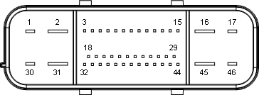
Table 2.1. Part numbers of the mating connector
| Supplier | Part number | Part |
|---|---|---|
| TE | 1326110-1 | Cable mount connector (right handed) |
| 1326341-1 | Cable mount connector (left handed) | |
| 1326113-1 | Cover |
Table 2.3. Part numbers for the 2.8 mm pin
| Supplier | Part number | Colour | Part |
|---|---|---|---|
| TE | 1326032-4 | Tin | Female crimp contact |
| Yazaki | 7158-3111-60 | Green | Seal (for wire 1.19 mm - 1.90 mm) |
| 7158-3112-70 | Yellow | Seal (for wire 1.88 mm - 2.10 mm) | |
| 7158-3113-40 | White | Seal (for wire 2.18 mm - 3.00 mm) | |
| 7158-3114-90 | Blue | Plug for unused position | |
| Pins A1, A17, A30 and A46 | |||
Table 2.5. Part numbers of the pin crimp tools
| Supplier | Tool assembly part number | Die assembly part number | Part |
|---|---|---|---|
| TE | 91338-1 | 91338-2 | Crimp tool for the 0.64 mm female terminal, PRO-CRIMPER III Hand Tool |
| Diamond Die and Mold Company | 088BR | - | Crimp tool for the 2.8 mm female terminal |
| 088BR-1 | Crimp tool for the 6.3 mm female terminal |
Table 2.6. Connector pinout — Pocket A
| Main connector — Pocket A | ||||||||
|---|---|---|---|---|---|---|---|---|
| Pin | P | Function | I/O | M | Loading | Filter | Range | Notes |
| A1 | Digital | O | Y | Low side | 1.5A | Related to internal channels Monitor (tt) and Monitor (v). | ||
| A2 | VPWR | P | 16 A | Related to internal channels AIN VPWR and DOT hold-PSU. | ||||
| A3 | Variable Resistance | O | Y | to VGND | 3.9 Ohm to 200.1 Ohm | Controlled by SPI. Related to internal channels DOT fault-clear and Monitor (ct). | ||
| A4 | Analogue | I | 51k to VGND plus 20k series | 530 Hz | 0V to 5V | General purpose analogue input. | ||
| A5 | Analogue | I | 51k to VGND plus 20k series | 530 Hz | 0V to 5V | General purpose analogue input. | ||
| A6 | Digital | I | 51k to VGND plus 47k series | 72Hz | 0V to VPWR | High-speed digital input associated with output pin A32. Active low. | ||
| A7 | Digital | I | 51k to VGND plus 47k series | 72 Hz | 0V to VPWR | High-speed digital input associated with output pin A33. Active low. | ||
| A8 | Digital | I | 51k to VGND plus 47k series | 72 Hz | 0V to VPWR | High-speed digital input associated with output pin A34. Active low. | ||
| A9 | Digital | I | 51 to VGND plus 47k series | 72 Hz | 0V to VPWR | High-speed digital input associated with output pin A35. Active low. | ||
| A10 | Digital | I | 4k7 to VPWR plus 47k series | 72 Hz | 0V to VPWR | High-speed digital input associated with output pin A36. Active low. | ||
| A11 | Digital | I | 4k7 to VPWR plus 47k series | 72 Hz | 0V to VPWR | High-speed digital input associated with output pin A37. Active low. | ||
| A12 | Digital | I | 51k to VGND plus 20k series | 530 Hz | 0V to VPWR | High-speed digital input associated with output pin A38. Active low. | ||
| Analogue | 0V to 5V | General purpose analogue input. | ||||||
| A13 | Digital | I | 15k to VPSU1 plus 20k series | 530 Hz | 0V to VPWR | High-speed digital input associated with output pin A39. Active low. | ||
| Analogue | 0V to 5V | General purpose analog input. | ||||||
| A14 | Digital | I | 51k to VGND plus 20k series | 530 Hz | 0V to VPWR | High-speed digital input associated with output pin A16. Active low. | ||
| Analogue | 0V to 5V | General purpose analogue input. | ||||||
| A15 | Digital | I | 200 ohm to VPSU1 plus 20k series | 530Hz | 0V to VPSU1 | High-speed digital input associated with output pin A45. Active low. | ||
| Analogue | 0V to 5V | General purpose analogue input. | ||||||
| A16 | Digital | O | Y | Low side | 4A peak / 1A hold | Related to internal channels DIN injector-batt-fault, DOT injector-clock, Monitor (d), Monitor (sb) and Monitor (v). | ||
| A17 | Digital | O | Y | Low side | 1.5A | Related to internal channels Monitor (tt) and Monitor (v). | ||
| A18 | Analogue | I | 15k to VPSU1 plus 20k series | 530 Hz | 0V to 5V | General purpose analogue input. | ||
| A19 | Analogue | I | 15k to VPSU1 plus 20k series | 530 Hz | 0V to 5V | General purpose analogue input. | ||
| A20 | Analogue | I | 51k to VGND plus 20k series | 530 Hz | 0V to 5V | General purpose analogue input. | ||
| A21 | Analogue | I | 51k to VGND plus 20k series | 530 Hz | 0V to 5V | General purpose analogue input. | ||
| A22 | Analogue | I | 1k to VPSU1 plus 20k series | 530 Hz | 0V to 5V | General purpose analogue input. | ||
| A23 | CAN+ (high) | No termination resistor | CAN bus 1 high (+ve), see also: A24. Related to internal channel DOT disable-CAN. | |||||
| A24 | CAN- (low) | No termination resistor | CAN bus 1 low (-ve), see also: A23. Related to internal channel DOT disable-CAN. | |||||
| A25 | Sensor Supply | P | Y | 5V, 250mA | Sensor supply 1. ±6% worst-case voltage tolerance. Related to internal channels DOT enable-EXT-PSU1 and Monitor (v). | |||
| A26 | Digital | I | 51k to VGND plus 47k series | 72Hz | 0V to VPWR | General purpose digital input / key position (ignition sense) input. | ||
| Analogue | 0V to 5V | General purpose analog input. | ||||||
| A27 | FEPS | I | 33k effective to VGND | 72Hz | -41V to +42V | Module flash programming control. General purpose digital input. Related to internal channel AIN FEPS. | ||
| Digital | 51k to VGND plus 47k series | 0V to VPWR | General purpose digital input. Related to internal channel AIN FEPS. | |||||
| A28 | CAN+ (high) | No termination resistor | CAN bus 0 high (+ve), see also: A43. Related to internal channel DOT disable-CAN. | |||||
| A29 | Digital | I | 4k7 to VPWR plus 47k series | 72Hz | 0V to VPWR | General purpose digital input. | ||
| A30 | Digital | O | Y | Low side | 1.5A | Related to internal channels Monitor (tt) and Monitor (v). | ||
| A31 | VGND | P | 16 A | |||||
| A32 | Digital | O | Y | Low side | 4A peak / 1A hold | Controlled directly by pin A6. Related to internal channels DIN injector-batt-fault, DOT injector-clock, Monitor (d), Monitor (sb) and Monitor (v). | ||
| A33 | Digital | O | Y | Low side | 4A peak / 1A hold | Controlled directly by pin A7. Related to internal channels DIN injector-batt-fault, DOT injector-clock, Monitor (d), Monitor (sb) and Monitor (v). | ||
| A34 | Digital | O | Y | Low side | 4A peak / 1A hold | Controlled directly by pin A8. Related to internal channels DIN injector-batt-fault, DOT injector-clock, Monitor (d), Monitor (sb) and Monitor (v). | ||
| A35 | Digital | O | Y | Low side | 4A peak / 1A hold | Controlled directly by pin A9. Related to internal channels DIN injector-batt-fault, DOT injector-clock, Monitor (d), Monitor (sb) and Monitor (v). | ||
| A36 | Digital | O | Y | Low side | 4A peak / 1A hold | Controlled directly by pin A10. Related to internal channels DIN injector-batt-fault, DOT injector-clock, Monitor (d), Monitor (sb) and Monitor (v). | ||
| A37 | Digital | O | Y | Low side | 4A peak / 1A hold | Controlled directly by pin A11. Related to internal channels DIN injector-batt-fault, DOT injector-clock, Monitor (d), Monitor (sb) and Monitor (v). | ||
| A38 | Digital | O | Y | Low side | 4A peak / 1A hold | Controlled directly by pin A12. Related to internal channels DIN injector-batt-fault, DOT injector-clock, Monitor (d), Monitor (sb) and Monitor (v). | ||
| A39 | Digital | O | Y | Low side | 4A peak / 1A hold | Controlled directly by pin A13. Related to internal channels DIN injector-batt-fault, DOT injector-clock, Monitor (d), Monitor (sb) and Monitor (v). | ||
| A40 | Sensor ground | P | 1 A | A40 and A31 connected together internally. | ||||
| A41 | Digital | I | 4k7 to VPWR plus 47k series | 72Hz | 0V to VPWR | General purpose digital input. | ||
| A42 | Digital | I | 4k7 to VPWR plus 47k series | 72Hz | 0V to VPWR | General purpose digital input. | ||
| A43 | CAN- (low) | No termination resistor | CAN bus 0 low (-ve), see also: A28. Related to internal channel DOT disable-CAN. | |||||
| A44 | Digital | I | 4k7 to VPWR plus 47k series | 50Hz | 0V to VPWR | General purpose digital input. | ||
| Analogue | 0V to 5V | General purpose analog input. | ||||||
| A45 | Digital | O | Y | Low side | 4A peak / 1A hold | Related to internal channels DIN injector-batt-fault, DOT injector-clock, Monitor (d), Monitor (sb) and Monitor (v). | ||
| A46 | Digital | O | Y | Low side | 1.5A | Related to internal channels Monitor (tt) and Monitor (v). | ||
Table 3.1. Internal signals
| Signal | I/O | Signal type | Range | Notes |
|---|---|---|---|---|
| Analogue | ||||
| AIN 3.3V | I | Analogue | 0V to 5V | Internal 3.3V supply monitor. 12-bit unsigned conversion. |
| AIN 5VD | I | Analogue | 0V to 5V | 5VD Reference voltage measurement. 12-bit unsigned conversion. |
| AIN FEPS (pin A27) | I | Analogue | -41.000V to +42.273V | Scaling from measured volts (Vm) to actual volts (Va) is Va = (1832*Vm-4510)/110. |
| AIN internal-ecu-temp | I | Analogue | -55 °C to 150 °C | Internal temperature monitor. 12-bit unsigned conversion. Transfer function is nonlinear and must be determined by lookup table. |
| AIN PSU+2.5VD | I | Analogue | 0V to 5V | Internal 2.5V precision reference. 12-bit unsigned conversion. |
| AIN VPWR (pin A2) | I | Analogue | 0V to 40V | Switched power supply voltage monitor. 12-bit unsigned conversion. To convert measured voltage (Vm) to actual voltage (Va) use the equation, Va=Vm*8. |
| AIN VREF | I | Analogue | 0V to 5V | Analogue input reference voltage measurement. 12-bit unsigned conversion. |
| AIN VRH | I | Analogue | 0V to 5V | 5V reference for analogue input conversions. 12-bit unsigned conversion. |
| AIN VRH-VRL 25% | I | Analogue | 0V to 5V | 1.25V reference for analogue input conversions. 12-bit unsigned conversion. |
| AIN VRH-VRL 50% | I | Analogue | 0V to 5V | 2.5V reference for analogue input conversions. Will read as 2.48V due to 20mV offset in processor implementation. 12-bit unsigned conversion. |
| AIN VRH-VRL 75% | I | Analogue | 0V to 5V | 3.75V reference for analogue input conversions. 12-bit unsigned conversion. |
| AIN VRL | I | Analogue | 0V to 5V | 0V reference for analogue input conversions. 12-bit unsigned conversion. |
| Current trip monitor | ||||
| Monitor (ct) (pin A3) | I | Digital | 0 or 1 | Active high. |
| Digital | ||||
| DIN injector-batt-fault (pin A16, A32, A33, A34, A35, A36, A37, A38, A39 and A45) | I | Digital | 0 or 1 | Batch fault indicator for injector outputs. Set to 1 when a short to battery fault occurs on any output. |
| DOT disable-CAN (pin A23 and A24) | O | Digital | 0 or 1 | Set to 0 to enable the CAN-1 transceiver, set to 1 to disable. |
| DOT disable-CAN (pin A28 and A43) | O | Digital | 0 or 1 | Set to 0 to enable the CAN-0 transceiver, set to 1 to disable. Implements Wake-On-CAN. |
| DOT enable-EXT-PSU1 (pin A25) | O | Digital | 0 or 1 | Sensor supply switch. Set to 1 to enable supply. |
| DOT fault-clear (pin A3) | O | Digital | 0 or 1 | A transition from 0 to 1 clears the current trip fault on the variable resistance output. |
| DOT hold-PSU (pin A2) | O | Digital | 0 or 1 | Control power supply to the ECU. |
| DOT injector-clock (pin A16, A32, A33, A34, A35, A36, A37, A38, A39 and A45) | O | Digital | 0 or 1 | PWM clock signal for all injectors. |
| Digital monitor | ||||
| Monitor (d) (pin A16) | I | Digital | 0 or 1 | Digital diagnostic monitor. |
| Monitor (d) (pin A32) | I | Digital | 0 or 1 | Digital diagnostic monitor. |
| Monitor (d) (pin A33) | I | Digital | 0 or 1 | Digital diagnostic monitor. |
| Monitor (d) (pin A34) | I | Digital | 0 or 1 | Digital diagnostic monitor. |
| Monitor (d) (pin A35) | I | Digital | 0 or 1 | Digital diagnostic monitor. |
| Monitor (d) (pin A36) | I | Digital | 0 or 1 | Digital diagnostic monitor. |
| Monitor (d) (pin A37) | I | Digital | 0 or 1 | Digital diagnostic monitor. |
| Monitor (d) (pin A38) | I | Digital | 0 or 1 | Digital diagnostic monitor. |
| Monitor (d) (pin A39) | I | Digital | 0 or 1 | Digital diagnostic monitor. |
| Monitor (d) (pin A45) | I | Digital | 0 or 1 | Digital diagnostic monitor. |
| Fault Monitor | ||||
| Monitor (sb) (pin A16) | I | Digital | 0 or 1 | Short to Battery fault monitor. Serial input. |
| Monitor (sb) (pin A32) | I | Digital | 0 or 1 | Short to Battery fault monitor. Serial input. |
| Monitor (sb) (pin A33) | I | Digital | 0 or 1 | Short to Battery fault monitor. Serial input. |
| Monitor (sb) (pin A34) | I | Digital | 0 or 1 | Short to Battery fault monitor. Serial input. |
| Monitor (sb) (pin A35) | I | Digital | 0 or 1 | Short to Battery fault monitor. Serial input. |
| Monitor (sb) (pin A36) | I | Digital | 0 or 1 | Short to Battery fault monitor. Serial input. |
| Monitor (sb) (pin A37) | I | Digital | 0 or 1 | Short to Battery fault monitor. Serial input. |
| Monitor (sb) (pin A38) | I | Digital | 0 or 1 | Short to Battery fault monitor. Serial input. |
| Monitor (sb) (pin A39) | I | Digital | 0 or 1 | Short to Battery fault monitor. Serial input. |
| Monitor (sb) (pin A45) | I | Digital | 0 or 1 | Short to Battery fault monitor. Serial input. |
| Memory check | ||||
| Monitor (counter eTPU background task) | I | Digital data | 0 to 65535 | Cyclic counter providing number of times the eTPU background task runs. Its rate of increase can be used to determine the rate of the background task. |
| Monitor (fc SDM-checksum) | I | Digital data | 0 to 65535 | Saturating counter providing number of times the eTPU module's data memory failed a checksum test. |
| Thermal trip monitor | ||||
| Monitor (tt) (pin A1) | I | Analogue | 0V to 5V | Digital output thermal trip monitor. |
| Monitor (tt) (pin A17) | I | Analogue | 0V to 5V | Digital output thermal trip monitor. |
| Monitor (tt) (pin A30) | I | Analogue | 0V to 5V | Digital output thermal trip monitor. |
| Monitor (tt) (pin A46) | I | Analogue | 0V to 5V | Digital output thermal trip monitor. |
| Voltage monitor | ||||
| Monitor (v) (pin A1) | I | Analogue | 0V to 36.915V | Digital output voltage monitor. 12-bit unsigned conversion. |
| Monitor (v) (pin A16) | I | Analogue | 0V to 7.5V | Injector diagnostic feedback voltage. |
| Monitor (v) (pin A17) | I | Analogue | 0V to 36.915V | Digital output voltage monitor. 12-bit unsigned conversion. |
| Monitor (v) (pin A25) | I | Analogue | 0V to 5.712V | Switched sensor supply voltage monitor. 12-bit unsigned conversion. To convert measured voltage (Vm) to actual voltage (Va) use the equation, Va=Vm*37.7/33. |
| Monitor (v) (pin A30) | I | Analogue | 0V to 36.915V | Digital output voltage monitor. 12-bit unsigned conversion. |
| Monitor (v) (pin A32) | I | Analogue | 0V to 7.5V | Injector diagnostic feedback voltage. |
| Monitor (v) (pin A33) | I | Analogue | 0V to 7.5V | Injector diagnostic feedback voltage. |
| Monitor (v) (pin A34) | I | Analogue | 0V to 7.5V | Injector diagnostic feedback voltage. |
| Monitor (v) (pin A35) | I | Analogue | 0V to 7.5V | Injector diagnostic feedback voltage. |
| Monitor (v) (pin A36) | I | Analogue | 0V to 7.5V | Injector diagnostic feedback voltage. |
| Monitor (v) (pin A37) | I | Analogue | 0V to 7.5V | Injector diagnostic feedback voltage. |
| Monitor (v) (pin A38) | I | Analogue | 0V to 7.5V | Injector diagnostic feedback voltage. |
| Monitor (v) (pin A39) | I | Analogue | 0V to 7.5V | Injector diagnostic feedback voltage. |
| Monitor (v) (pin A45) | I | Analogue | 0V to 7.5V | Injector diagnostic feedback voltage. |
| Monitor (v) (pin A46) | I | Analogue | 0V to 36.915V | Digital output voltage monitor. 12-bit unsigned conversion. |
- 4.1. ECU power
- 4.2. ECU power — control
- 4.3. ECU power — sensor supplies
- 4.4. Analogue inputs
- 4.5. Analogue inputs — ratiometric measurement
- 4.6. Analogue inputs — internal temperature input
- 4.7. Analogue inputs — relationship between VREF, sensor supplies and inputs
- 4.8. Digital inputs
- 4.9. Digital outputs
- 4.10. Digital output — state monitoring
- 4.11. Digital output — low-side driver protection and diagnostics
- 4.12. Injector outputs — operation
- 4.13. Injector outputs — open circuit and short-to-ground diagnostics
- 4.14. Injector outputs — short-to-battery diagnostics
- 4.15. Variable resistance output — operation
- 4.16. Variable resistance output — over current protection
- 4.17. CAN communication busses
- 4.18. Memory — non-volatile storage and lifetime
- 4.19. System modes
- 4.20. Floating point capabilities
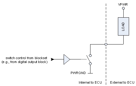
The power supply pin (VPWR A2) and the ground pin (VGND A31) are both rated to (pending).
The ECU VGND (pin A31) and sensor ground (pins A40) are directly connected together via a ground plane in the ECU PCB. The ECU case is capacitively coupled to VGND.
The ECU is designed for 12V or 24V vehicles, with various modes of operation based on the voltage (see Table 1.1, “Specification”). The ECU is protected against reverse supply connection. All inputs and outputs are protected against short-to-VPWR or short-to-VGND over normal operating range.
The ECU power arrangement is shown in Figure 4.1, “Switching arrangement for main power supply”.
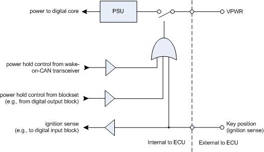
In order to power the ECU from a sleep state, the power supply pin (VPWR A2) must be powered and at least one of the following must occur:
The ECU will remain powered as long as the power supply pin (VPWR A2) is connected to a power supply and any one of the following signals are asserted:
key position (ignition sense) input (pin A26)
the internal power hold signal (DOT hold-PSU)
the CAN transceiver on pins A28 and A43 has detected CAN traffic
Note
In order for the ECU to enter a shutdown state, all three signals must be non-asserted.
In order to shut the ECU down, the CAN transceiver on pins A28 and A43 must be placed into its shutdown state. To place the transceiver into its shutdown state, the DOT disable-CAN must be toggled at a frequency of 1 Hz and a duty cycle of 50%.
Note
If there is any CAN traffic on this CAN bus, however, the ECU will not be able to enter a shutdown state.
The application software must monitor the CAN bus and determine if it is appropriate to shut the ECU down by disabling the CAN transceiver.
The internal power hold signal allows for the ECU application software to hold the ECU on after the external key position input is opened, allowing, for example, non-volatile memory processing to occur. For the ECU to hold power the internal DOT hold-PSU channel needs to be asserted. Setting this internal channel high will hold power when the key position input is opened, setting it low will allow the ECU to power off when the key position input is opened.
Note
When using the power hold functionality, it is best to set the internal DOT hold-PSU channel high as soon as the external key position input (pin A26) is closed and only set low once all required shutdown tasks have completed.
Note
When the ECU is first connected to a power supply, the ECU will power itself up regardless of the state of the external key position input even if there is no CAN traffic due to the initialization behavior of the wake-on-CAN device.
If there is no application software, the boot code will place the ECU into a shutdown state after 10 seconds of inactivity on the CAN bus.
The ECU provides one external sensor power supply (pin A25). The sensor supply can be switched off using DOT enable-EXT-PSU1 to allow the application software to perform intrusive diagnostics on sensors.
The power supply is monitored by an analogue input which can be used to check for short circuits and measure the exact output voltage for use with ratiometric sensors.
The analogue inputs (pins A4, A5, A15, A18, A19, A20, A21 and A22) sample voltage with varying resolution and range. See the pin information for more details.
Note
If any of the pins A16, A32, A33, A34, A35, A36, A37, A38, A39 and A45 are not being used as digital outputs then it is possible for them to be used as analogue inputs with a range of 0V to 7.5V, a loading of TBC to ground and a filter of 1Hz.
If any of the pins A1, A17, A30 and A46 are not being used as digital outputs then it is possible for them to be used as analogue inputs with a range of 0V to 36.915V, a loading of 47K to ground and a filter of 78Hz.
Providing the output transistor is switched off, the pin can be driven by an external source and the pin's voltage monitor will reflect the actual voltage on the pin.
Ratiometric sensors are read in as a ratio between the sensor and reference voltages (Vsens/Vref). Correction is only required on channels for which an absolute voltage measurement is required. Correction is not required for sensors supplied from the 5V sensor supply and which produce an output that is ratiometric to the supply.
To read a variable sensor which is an absolute referenced sensor (Vsens,abs) the Vref for the ADC requires correction:
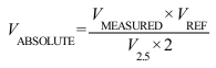
Where VMEASURED is the A/D conversion for an external pin, VREF is the A/D conversion for internal channel AIN VRH, V2.5 is the A/D conversion for internal channel AIN PSU+2.5VD, and 2 is a constant.
The M221 family has provision for an internal temperature sensor measured by AIN internal-ecu-temp. This temperature sensor is unpopulated by default, so measurements of this signal will report 0 V.
The ECU power arrangement is shown in Figure 4.2, “VREF arrangement”. The figure shows the relationship between the internal 5V VREF and ground, the external sensor supply and ground, and the analogue inputs.
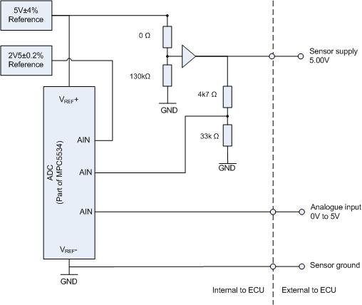
The internal low precision 5V reference supplies the reference pin on the ADC. The exact voltage being produced can be read on a scaled ADC channel, Vext_psu = (Vadc * 37.7)/33. The sensor ground is a nominal 0V, but may be slightly above this due to voltage drop across the protection device.
The exact voltage on the analogue input pin can be read on a direct (unscaled) ADC channel. Standard 0-5V inputs are passed directly to the ADC with no scaling.
Some analogue input pins are internally pulled up to the sensor power supply (pin A25). If the sensor supply is not enabled, floating inputs will fluctuate when read by the ADC. The sensor supply must be enabled for voltage measurements made on any of these channels.
The digital inputs (pins A6, A7, A8, A9, A10, A11, A12, A13, A14, A15, A26, A27, A29, A41, A42 and A44) sense the binary state based on the pin voltage and a threshold.
- Not inverted
For pins A12, A13, A14, A26, A29, A41, A42 and A44, see Table 4.2, “Digital input thresholds” for input voltages corresponding to the measured digital state.
- Inverted
The M221 injector trigger inputs A6, A7, A8, A9, A10, A11, A12, A13, A14 and A15 inputs are inverted digital inputs. See Table 4.3, “Injector trigger input thresholds” for the voltage thresholds on these inputs.
Note
All external signals are low pass filtered to prevent signals of excessive frequency from tying up the target processor. See the pin information for more details.
Pins A1, A17, A30 and A46 are configured as low-side — the ECU switches the output pin to ground, the load is connected to the output pin and the battery.
These low-side digital outputs contain internal monitoring circuitry that provides diagnostic information. However, as a consequence a small leakage current will flow through the actuator when the low-side output driver is turned off. Refer to Table 4.4, “Low-side digital output leakage current” for typical leakage currents at specified operating voltages.
Table 4.4. Low-side digital output leakage current
| Supply Voltage (V) | Typical Leakage Current (mA) |
|---|---|
| 13 | 0.030 |
| 25 | 0.075 |
The voltage of the digital output pins A1, A17, A30 and A46 can be monitored using a corresponding internal Monitor (v) channel. The analogue monitor channel measures the actual voltage at the pin after scaling according to the equation
measured voltage (Vm, 0 to 5V) to actual voltage (Va, 0 to 36.9V): Va = Vm*347/47
When the pin is used as a PWM, there are two possible uses for such a feedback:
Before starting a PWM, by reading the voltage on the pin and checking for open or short circuits.
By reading the average voltage on a PWM output and comparing it with the demanded PWM width and the battery voltage reading, you can perform a consistency check that the PWM output is performing as expected. This method can be applied if the PWM frequency is higher than the filter cut off frequency for that output.
When the pin is used as a plain digital output, feedback is used as follows:
Read the voltage on the pin and check for open or short circuits.
The digital outputs A1, A17, A30 and A46 are self protected by a thermal shutdown circuit. This protection is based only on output driver chip temperature and is independent of operating voltage.
Over-temperature shutoff occurs in the range 150 to 190 ºC (170 ºC typical). The device automatically restarts when temperature falls approximately 15 ºC below cutoff temperature.
An application can monitor these outputs for thermal shutdown via the Monitor (tt) analogue input channels for the corresponding outputs. See Table 4.5, “Low-side digital output thermal trip” for threshold values.
Table 4.5. Low-side digital output thermal trip
| Monitor (tt) voltage | Output Status |
|---|---|
| <= 1 V | Device in thermal shutdown |
| >= 4.7 V | Normal operation |
Note
The low-side output thermal monitors are non-latching; in order to guarantee detection of a fault, the application must balance the rate at which it samples the monitor inputs against the cooldown rate of the hardware in a fault condition. This rate will depend on the particular installation and usage profile of the ECU, but in general higher sample rates are required for cooler environmental conditions.
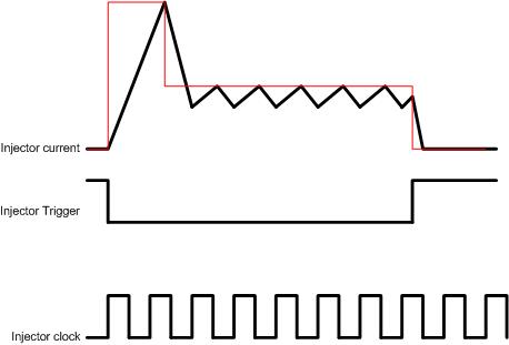
The injector outputs (pins A16, A32, A33, A34, A35, A36, A37, A38, A39 and A45) are peak and hold injectors controlled by the associated injector trigger inputs A6, A7, A8, A9, A10, A11, A12, A13, A14 and A15 and the injector clock controlled by PWM output DOT injector-clock.
The application must set the DOT injector-clock output to the desired dither frequency and 50% duty cycle for proper operation.
When a trigger input pin for an injector transitions from high to low, the associated injector output will be turned on. The output current will be allowed to rise to the peak current of 4A, then will immediately be limited to the hold current of 1A. See Figure 4.4, “Normal injector operation” for the normal operation waveform. See Table 4.6, “Injector current thresholds” for the range of peak and hold currents.
Note
If an injector output is short-to-battery, the current waveform will essentially be the same as the normal operation waveform.
Note
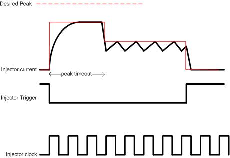
If the current does not reach the peak current within nominal 7 ms (due to, for instance, low supply voltage), the output will switch to the 1A hold level. This timeout may be different under option control; consult option control documentation if applicable. See Figure 4.5, “Injector operation under timeout”
The injector trigger input must be high for at least (pending) ms to re-enable the peak current threshold after an output is switched off.
The injector outputs (A16, A32, A33, A34, A35, A36, A37, A38, A39 and A45) include output state and short-to-battery monitors.
The digital and analogue state monitors Monitor (d), Monitor (v), respectively, for the injector output pins reflect the state of the output pin. A short to ground or open-circuit condition is indicated if the Monitor (d) remains zero or the Monitor (v) remains below a threshold. See Table 4.7, “Injector Diagnostic Monitor(v) thresholds” for threshold levels.
Table 4.7. Injector Diagnostic Monitor(v) thresholds
| Monitor (v) voltage | Output Status |
|---|---|
| >= 3.41 V | Normal |
| <= 2.42 V | Open or shorted to ground |
The M221 injector output hardware monitors the outputs for short to battery operation. This detection requires an injector to be activated, and the hardware latches the first detected fault until the application reads the fault flag status. The faults are made available by reading the Monitor (sb) digital inputs (see Table 4.8, “Injector Diagnostic Monitor(sb) levels”). The platform will set the DIN injector-batt-fault digital input to 1 when a new injector short-to-battery fault has been detected.
An application should read the Monitor (sb) digital inputs at a fast rate to ensure that it detects all occurrences of faults on each injector. If a short-to-battery fault is detected on one injector, no other injectors can register a fault until that first fault is read by the application.
Reading the Monitor (sb) input for an injector will reset the fault flag for that output as well as the DIN injector-batt-fault fault flag.
Note
Reading a Monitor (sb) flag to clear the DIN injector-batt-fault has a delay of one model iteration; if the application reads a short to battery monitor in one iteration and the DIN injector-batt-fault is asserted at the beginning of the next iteration, a new injector fault has been detected.
The injector short to battery protection acts as a current limit; the output will still be active as long as the input trigger pin is low but the current will be limited to the hold current of 1A.
Table 4.8. Injector Diagnostic Monitor(sb) levels
| Monitor (sb) value | Output Status |
|---|---|
| 1 | Normal |
| 0 | Short to battery |
The M221 provides a variable resistance output on A3.
The resistance is controlled by using a SPI based digital potentiometer. The output of the digital potentiometer is controlled from software by commanding it to a percentage of its total range. The digital potentiometer resistance is calculated according to the following transfer function:
Digital potentiometer resistance = (50000 Ohm * commanded percentage) + wiper resistance
Where the wiper resistance is between 50 and 100 Ohm.
The overall circuit resistance is then calculated according to the following equation:
resistance = (50300 / (Digital potentiometer resistance)) * 3.9 Ohm + 3.9 Ohm.
The output is protected for over-current. If the current through the effective resistance exceeds approximately 1A, the hardware will assert the Monitor (ct) digital input and set the input to its maximum resistance.
If the current trip is asserted, the application should reduce the digital poteniometer resistance to its minimum (highest circuit resistance), then set the DOT fault-clear to one to re-enable the output.
Note
The DOT fault-clear signal is edge-based; the fault condition is cleared on a transition of this signal from 0 to 1. If the short condition is persistent, however, the Monitor (ct) will immediately set again, and an application must set the fault clear flag to zero again before attempting to reset the output.
The CAN busses (pins A23+A24 and A28+A43) are implemented using high-speed CAN transceivers. Neither CAN bus has terminating resistors.
CAN bus 0 (pins A28+A43) will wake the ECU from shutdown mode if traffic is detected on that bus.
The ECU supports non-volatile memory storage in Flash. Battery backed RAM is not supported.
The processor's Flash memory is split into small and large memory blocks. The application and calibration are stored in large blocks, whilst DTC information, freeze frames and so on are stored in small blocks.
The largest Flash block can take up to approximately 7.5 seconds to erase. This occurs in an environment where the Flash has been erased and programmed many times at its temperature extreme. The typical erase time is smaller, especially at ambient temperatures. Reprogramming an ECU (where many large blocks would be erased), or storing DTC information across power cycles, can therefore take some time. Users and applications should take this into consideration.
The minimum number of erase cycles is approximately 1,000 for large Flash blocks and 100,000 for small Flash blocks. This occurs in an environment where the Flash has been erased and programmed many times at its temperature extreme. The typical number of erase cycles is larger, especially at ambient temperatures.
The minimum data retention is approximately 5 years for blocks which have been erased less than 100,000 times, and approximately 20 years for blocks which have been erased less than 1,000 times.
The information about the Flash has been taken from Freescale's MPC5534 Microcontroller Data Sheet document, revision 4 (dated Mar 2008).
The ECU can run in one of two system modes: reprogramming mode and application mode. In reprogramming mode, the ECU can be reprogrammed with application software from a calibration tool. In application mode, the ECU runs the programmed application software. The ECU selects which mode to enter when it is powered up by measuring the voltage on the A27 pin.
Table 4.9. System mode selection
| Voltage | System mode |
|---|---|
| > +36V | Enter reprogramming mode. If valid application software has previously been programmed, then use the CCP settings from that application, otherwise use the default CCP settings. |
| < -16V | Enter reprogramming mode. Use the default CCP settings. |
| Otherwise | Enter application mode if valid application software has previously been programmed, otherwise enter reprogramming mode. |
The ECU closely adheres to the IEEE-754 for floating point numbers.
When using Simulink, floating point Simulink models are supported — all calculations are performed using single-precision (even if the model uses double-precision, the ECU performs calculations using single-precision).
When using the C-API, floating point applications are supported — all calculations are performed using single or double precision, as determined by the application code (although double precision will incur some software overhead — see the compiler reference manual for further details).
The rounding mode is set to round-to-nearest. In some conditions, the ECU will not adhere to the IEEE-754 standard:
Table 4.10. Floating point conditions
| Condition | Result |
|---|---|
| Underflow | The result of a calculation underflow is ±0. The sign is based on the signs of the operands. |
| Overflow | The result of a calculation overflow is ±max where max is approximately 3.4 × 1038. The sign is based on the signs of the operands. |
| Divide by zero |
The ECU does not generate ±Inf, NaN or a denormalised number as the result of a calculation.
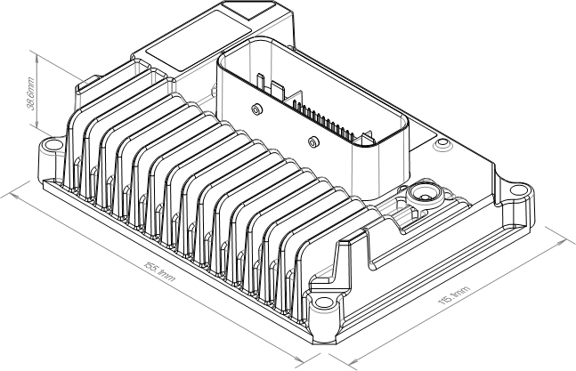
The ECU has the following dimensions:
If you have questions, or are experiencing issues with OpenECU please see the FAQ website:
- website
If you still have questions after searching through the FAQ, or want to discuss sales or proposals, you can contact main office:
- Tel
- +1 734 656 0140
- Fax
- +1 734 656 0141
during normal working hours (Mon to Fri, 0930 to 1700 EST).