Release 2.9.0 (r2020-1)
Copyright © 2020 Pi Innovo
13-Apr-2020
Table of Contents
- 1. Technical specification
- 2. Connector pinout
- 3. Internal signals
- 4. Operational details
- 4.1. ECU power
- 4.2. ECU power — control
- 4.3. ECU power — actuator supplies
- 4.4. ECU power — sensor supplies
- 4.5. Analogue inputs
- 4.6. Analogue inputs — internal temperature input
- 4.7. Analogue inputs — internal accelerometer inputs
- 4.8. Analogue inputs — internal gyroscope inputs
- 4.9. Analogue inputs — internal accelerometer and gyroscope orientation
- 4.10. Digital inputs
- 4.11. Digital outputs
- 4.12. Digital output — state monitoring
- 4.13. Digital output — driver protection
- 4.14. Serial inputs and outputs
- 4.15. Communication — CAN
- 4.16. Memory — configuration
- 4.17. Memory — non-volatile storage and lifetime
- 4.18. Memory — calibration capabilities
- 4.19. System modes
- 4.20. Flash codes
- 4.21. Calibration capabilities
- 4.22. Floating point capabilities
- 5. Dimensions
- A. Contact information
List of Figures
List of Tables
- 1.1. Specification
- 1.2. Function reference
- 2.1. Part numbers for the mating connector
- 2.2. Part numbers for the turned pin
- 2.3. Part numbers for the formed pin
- 2.4. Connector pinout — Pocket A
- 2.5. Part numbers for the mating connector
- 2.6. Part numbers for the turned pin
- 2.7. Part numbers for the formed pin
- 2.8. Connector pinout — Pocket C
- 3.1. Internal signals
- 4.1. Sensor supply monitor voltages
- 4.2. Sensor ground monitor voltage
- 4.3. Low-side digital output leakage current
- 4.4. Memory configurations supported
- 4.5. System mode selection
- 4.6. Flash code example
- 4.7. Flash codes
- 4.8. Floating point conditions
This document is the technical specification for OpenECU part 01T-068148-000 Issue 1. Within this document, that part is referred to as the M461-000 ECU.
Note
For a list of issues and possible work arounds for this ECU, found after publication of this document, please refer to the hardware errata for this ECU (named 29T-068148ER-xE M461 Technical Spec Errata ).
Specific option control may exist for this part. In that case, parts of this document will be overridden by an option control specific technical specification. Please refer to the option control technical specification for more information.
This technical specification relates to the following ECU variant:
M461D-000 — for development and testing, including full interactive calibration tool integration.
Table 1.1. Specification
| Specification | Variant |
|---|---|
| M461D-000 | |
| Status | Available [a] |
| Processor | MPC5534 |
| Rate | 80MHz |
| Code space | up to 768KiB [b] |
| RAM space | up to 832KiB [b] |
| Calibration space | up to 256KiB [b] |
| Calibratable | Y |
| Reprogrammable | Y |
| Power control relays | - |
| Actuator supplies | - |
| Sensor supplies | 4 |
| Inputs | 33 |
| Outputs | 14 |
| CAN buses | 2 |
| LIN buses | - |
| RS232 links | - |
| Connectors | 2x40 |
| Weight | 1.5Kg |
| Vibration | 6g random RMS |
| Shock capability | TBC |
| Enclosure | IP68 [c] |
| EMC | SAE J1455 [d] |
| Partial operating voltage | 7 to 36V |
| Full operating voltage | 8 to 32V [e] |
| Standby current (typical) | 0.15mA at 12V [f] |
| Operating current (typical) | 175mA at 12V [g] |
| Operating temperature range | -40 to +105°C |
| Storage temperature range (installation) | -40 to +125°C |
| Storage temperature range (shipping) | -40 to +125°C |
[a] Target ECU available for general use. [b] See list of possible memory configurations in section 'Memory - configuration'. [c] Designed for under bonnet(hood)/chassis mounting. [d] Load dump protection to SAE J1455 specification. [e] Designed for 12V or 24V vehicles. [f] 0.3mA at 24V. [g] 100mA at 24V. When running idle task with I/O disconnected. | |
Various input and output functionality is supported where some pins may be capable of more than one function. Some functions require a combination of pins but not all pin combinations are possible.
Table 1.2. Function reference
| I/O type | External | Internal | Pins |
|---|---|---|---|
| Power | |||
| ECU supply | 1 | - | A10+A20+A30 |
| ECU ground | 1 | - | C1+C2+C11+C12+C38 |
| Sensor supply | 4 | - | A8, A18, C8, C18 |
| Module control, status | |||
| Ignition sense | 1 | - | A12 |
| Module control FEPS | 1 | - | A2 |
| Module status Flash code | 1 | - | A27 |
| Communication | |||
| CAN buses | 2 | - | A37+A36, C37+C36 |
| Inputs — time based | |||
| Analogue | 23 | 36 | A16, A22, A23, A24, A28, A32, A33, A34, C3, C4, C6, C13, C14, C16, C21, C22, C23, C24, C25, C31, C32, C33, C35 |
| Digital | 10 | 26 | A12, A26, C7, C27, C28, C29, C30, C34, C39, C40 |
| Frequency | 10 | 13 | A12, A26, C7, C27, C28, C29, C30, C34, C39, C40 |
| PWM | 10 | - | A12, A26, C7, C27, C28, C29, C30, C34, C39, C40 |
| Quadrature | 9 | - | A26, C7, C27, C28, C29, C30, C34, C39, C40 |
| Outputs — time based | |||
| Digital | 14 | 7 | A1, A5, A7, A11, A15, A17, A21, A25, A31, A35, C5, C10, C15, C20 |
| PWM | 14 | - | A1, A5, A7, A11, A15, A17, A21, A25, A31, A35, C5, C10, C15, C20 |
| Inputs — angle based | |||
| None | - | - | |
| Outputs — angle based | |||
| None | - | - | |
The M461-000 variants have two ECU connectors (pockets) named A and C, which have pinouts as given in the following tables. Currents listed are RMS unless otherwise stated.
The following abbreviations are used in the pinout tables below:
C Communication I Input M Monitor O Output P Power
CT Current trip GND Ground PSU Power supply PWR Power RTD Resistance temperature detector
Connector packs can be ordered from Pi. Individual connector components can be ordered from Pi or from various manufacturers.
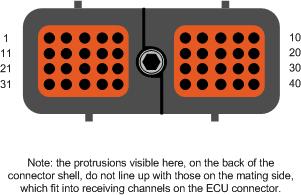
Table 2.1. Part numbers for the mating connector
| Supplier | Part number | Part |
|---|---|---|
| Deutsch | DRC26-40SA | Connector with A keyway |
Table 2.4. Connector pinout — Pocket A
| Main connector — Pocket A | ||||||||
|---|---|---|---|---|---|---|---|---|
| Pin | P | Function | I/O | M | Loading | Filter | Range | Notes |
| A1 | Digital | O | Y | Low side | 5A | Related to internal channels Monitor (ct), Monitor (d) and Monitor (v). | ||
| A2 | FEPS | I | 82k series with bias of 11k to VGND and 10k to 5V | 323Hz | -16V to +17V | Module flash programming control. | ||
| A3 | No function. | |||||||
| A4 | No function. | |||||||
| A5 | Digital | O | Y | Low side | 8A | Related to internal channels Monitor (ct), Monitor (d) and Monitor (v). | ||
| A6 | No function. | |||||||
| A7 | Digital | O | Y | Low side | 100mA | Related to internal channels Monitor (d) and Monitor (v). | ||
| A8 | Sensor supply | P | Y | 5V, 250mA | Sensor supply 1. Can be turned on and off by the application for diagnostics purposes, see also: A9. Related to internal channels DOT disable-EXT-PSU1 and Monitor (v). | |||
| A9 | Sensor ground | P | Sensor ground 1, see also: A8. Related to internal channel AIN extern-gnd. | |||||
| A10 | VPWR | P | 7A | Maximum of 21A in total when all VPWR pins connected in parallel. Related to internal channel AIN VPWR. | ||||
| A11 | Digital | O | Y | Low side | 5A | Related to internal channels Monitor (ct), Monitor (d) and Monitor (v). | ||
| A12 | Digital | I | 4k7 to VGND | 6.9kHz | 0V to VPWR | Key position (ignition sense) input. Related to internal channel DOT hold-PSU. | ||
| A13 | No function. | |||||||
| A14 | No function. | |||||||
| A15 | Digital | O | Y | Low side | 8A | Related to internal channels Monitor (ct), Monitor (d) and Monitor (v). | ||
| A16 | Analogue | I | 51k to VGND | 22Hz | 0V to 5V | 12-bit unsigned conversion. | ||
| A17 | Digital | O | Y | Low side | 100mA | Related to internal channels Monitor (d) and Monitor (v). | ||
| A18 | Sensor supply | P | Y | 5V, 250mA | Sensor supply 2. Can be turned on and off by the application for diagnostics purposes, see also: A19. Related to internal channels DOT disable-EXT-PSU2 and Monitor (v). | |||
| A19 | Sensor ground | P | Sensor ground 2, see also: A18. Related to internal channel AIN extern-gnd. | |||||
| A20 | VPWR | P | 7A | Maximum of 21A in total when all VPWR pins connected in parallel. Related to internal channel AIN VPWR. | ||||
| A21 | Digital | O | Y | Low side | 5A | Related to internal channels Monitor (ct), Monitor (d) and Monitor (v). | ||
| A22 | Analogue | I | 51k to VGND | 220Hz | 0V to 5V | 12-bit unsigned conversion. | ||
| A23 | Analogue | I | 51k to VGND | 220Hz | 0V to 5V | 12-bit unsigned conversion. | ||
| A24 | Analogue | I | 51k to VGND | 220Hz | 0V to 5V | 12-bit unsigned conversion. | ||
| A25 | Digital | O | Y | Low side | 8A | Related to internal channels Monitor (ct), Monitor (d) and Monitor (v). | ||
| A26 | Digital | I | 4k7 to VPWR through diode | 6.9kHz | 0V to VPWR | |||
| A27 | Flash code | O | Low side | 100mA | ECU status information. | |||
| A28 | Analogue | I | 51k to VGND | 42Hz | 0V to 5V | 12-bit unsigned conversion. | ||
| A29 | No function. | |||||||
| A30 | VPWR | P | 7A | Maximum of 21A in total when all VPWR pins connected in parallel. Related to internal channel AIN VPWR. | ||||
| A31 | Digital | O | Y | Low side | 5A | Related to internal channels Monitor (ct), Monitor (d) and Monitor (v). | ||
| A32 | Analogue | I | 51k to VGND | 220Hz | 0V to 5V | 12-bit unsigned conversion. | ||
| A33 | Analogue | I | 51k to VGND | 220Hz | 0V to 5V | 12-bit unsigned conversion. | ||
| A34 | Analogue | I | 51k to VGND | 220Hz | 0V to 5V | 12-bit unsigned conversion. | ||
| A35 | Digital | O | Y | Low side | 2A | Related to internal channels Monitor (ct), Monitor (d) and Monitor (v). | ||
| A36 | CAN+ (high) | C | 124R | CAN bus 0 high (+ve). | ||||
| A37 | CAN- (low) | C | 124R | CAN bus 0 low (-ve). | ||||
| A38 | CAN shield | C | CAN bus 0 shield. | |||||
| A39 | No function. | |||||||
| A40 | No function. | |||||||
Connector packs can be ordered from Pi. Individual connector components can be ordered from Pi or from various manufacturers.
Table 2.5. Part numbers for the mating connector
| Supplier | Part number | Part |
|---|---|---|
| Deutsch | DRC26-40SC | Connector with C keyway |
Table 2.8. Connector pinout — Pocket C
| Main connector — Pocket C | ||||||||
|---|---|---|---|---|---|---|---|---|
| Pin | P | Function | I/O | M | Loading | Filter | Range | Notes |
| C1 | VGND | P | C1, C2, C11, C12 and C38 connected together internally. | |||||
| C2 | VGND | P | C1, C2, C11, C12 and C38 connected together internally. | |||||
| C3 | Analogue (RTD) | I | 10k to 5V | 124Hz | 0V to 0.454545V | 12-bit unsigned conversion. | ||
| C4 | Analogue | I | 51k to VGND | 42Hz | 0V to 5V | 12-bit unsigned conversion. | ||
| C5 | Digital | O | Y | Low side | 2A | Related to internal channels Monitor (ct), Monitor (d) and Monitor (v). | ||
| C6 | Analogue | I | 51k to VGND | 42Hz | 0V to 5V | 12-bit unsigned conversion. | ||
| C7 | Digital | I | 36k to VGND | 6.9kHz | 0V to 5V | |||
| C8 | Sensor supply | P | Y | 5V, 250mA | Sensor supply 3. Can be turned on and off by the application for diagnostics purposes, see also: C9. Related to internal channels DOT disable-EXT-PSU3 and Monitor (v). | |||
| C9 | Sensor ground | P | Sensor ground 3, see also: C8. Related to internal channel AIN extern-gnd. | |||||
| C10 | Digital | O | Y | Low side | 2A | Related to internal channels Monitor (ct), Monitor (d) and Monitor (v). | ||
| C11 | VGND | P | C1, C2, C11, C12 and C38 connected together internally. | |||||
| C12 | VGND | P | C1, C2, C11, C12 and C38 connected together internally. | |||||
| C13 | Analogue (RTD) | I | 10k to 5V | 124Hz | 0V to 0.454545V | 12-bit unsigned conversion. | ||
| C14 | Analogue | I | 51k to VGND | 42Hz | 0V to 5V | 12-bit unsigned conversion. | ||
| C15 | Digital | O | Y | Low side | 8A | Related to internal channels Monitor (ct), Monitor (d) and Monitor (v). | ||
| C16 | Analogue | I | 51k to VGND | 22Hz | 0V to 5V | 12-bit unsigned conversion. | ||
| C17 | No function. | |||||||
| C18 | Sensor supply | P | Y | 5V, 250mA | Sensor supply 4. Can be turned on and off by the application for diagnostics purposes, see also: C19. Related to internal channels DOT disable-EXT-PSU4 and Monitor (v). | |||
| C19 | Sensor ground | P | Sensor ground 4, see also: C18. Related to internal channel AIN extern-gnd. | |||||
| C20 | Digital | O | Y | Low side | 2A | Related to internal channels Monitor (ct), Monitor (d) and Monitor (v). | ||
| C21 | Analogue (RTD) | I | 10k to 5V | 124Hz | 0V to 0.454545V | 12-bit unsigned conversion. | ||
| C22 | Analogue | I | 51k to VGND | 220Hz | 0V to 5V | 12-bit unsigned conversion. | ||
| C23 | Analogue | I | 51k to VGND | 220Hz | 0V to 5V | 12-bit unsigned conversion. | ||
| C24 | Analogue | I | 51k to VGND | 63Hz | 0V to 5V | Can be treated as an individual input, or as a differential input with C25. 12-bit unsigned conversion. Related to internal channel AIN diff.. | ||
| C25 | Analogue | I | 51k to VGND | 42Hz | 0V to 5V | Can be treated as an individual input, or as a differential input with C24. 12-bit unsigned conversion. Related to internal channel AIN diff.. | ||
| C26 | No function | This pin is directly tied internally to the analogue ground of the ECU. Care must be taken to protect from shorts to positive voltage in the wiring harness. | ||||||
| C27 | Digital | I | 4k7 to VPWR through diode plus 51k to VGND | 6.9kHz | 0V to VPWR | |||
| C28 | Digital | I | 4k7 to VPWR through diode | 6.9kHz | 0V to VPWR | |||
| C29 | Digital | I | 4k7 to VPWR through diode | 6.9kHz | 0V to VPWR | |||
| C30 | Digital | I | 4k7 to VPWR through diode | 6.9kHz | 0V to VPWR | |||
| C31 | Analogue | I | 51k to VGND | 42Hz | 0V to 5V | 12-bit unsigned conversion. | ||
| C32 | Analogue | I | 51k to VGND | 63Hz | 0V to 5V | 12-bit unsigned conversion. | ||
| C33 | Analogue | I | 51k to VGND | 63Hz | 0V to 5V | 12-bit unsigned conversion. | ||
| C34 | Digital | I | 4k7 to VPWR through diode | 6.9kHz | 0V to VPWR | |||
| C35 | Analogue | I | 51k to VGND | 42Hz | 0V to 5V | 12-bit unsigned conversion. | ||
| C36 | CAN+ (high) | C | 124R | CAN bus 1 high (+ve). | ||||
| C37 | CAN- (low) | C | 124R | CAN bus 1 low (-ve). | ||||
| C38 | VGND | P | C1, C2, C11, C12 and C38 connected together internally. | |||||
| C39 | Digital | I | 36k to VGND | 6.9kHz | 0V to VPWR | |||
| C40 | Digital | I | 36k to VGND | 0V to VPWR | ||||
Table 3.1. Internal signals
| Signal | I/O | Signal type | Range | Notes |
|---|---|---|---|---|
| Analogue | ||||
| AIN accelerometer-x | I | Analogue | 0V to 5V | Internal X-axis accelerometer signal. 12-bit unsigned conversion. |
| AIN accelerometer-y | I | Analogue | 0V to 5V | Internal Y-axis accelerometer signal. 12-bit unsigned conversion. |
| AIN accelerometer-z | I | Analogue | 0V to 5V | Internal Z-axis accelerometer signal. 12-bit unsigned conversion. |
| AIN cold-junction-temp | I | Analogue | 0V to 5V | Cold junction temperature: 0.251V @ -40°C; 1.31525V @ +125°C. 12-bit unsigned conversion. |
| AIN diff. (pin C24 and C25) | I | Analogue | 0V to 5V | Differential input. 12-bit unsigned conversion. |
| AIN extern-gnd (pin A9, A19, C9 and C19) | I | Analogue | 0V to 5V | Common sensor ground voltage monitor. 12-bit unsigned conversion. |
| AIN gyroscope-temperature | I | Analogue | 0V to 5V | Internal gyroscope temperature. 12-bit unsigned conversion. |
| AIN gyroscope-x | I | Analogue | 0V to 5V | Internal X-axis gyroscope signal. 12-bit unsigned conversion. |
| AIN gyroscope-y | I | Analogue | 0V to 5V | Internal Y-axis gyroscope signal. 12-bit unsigned conversion. |
| AIN gyroscope-z | I | Analogue | 0V to 5V | Internal Z-axis gyroscope signal. 12-bit unsigned conversion. |
| AIN PSU+3V3 | I | Analogue | 0V to 5V | Internal 3.3V power supply. 12-bit unsigned conversion. |
| AIN PSU+5VD | I | Analogue | 0V to 6V | Internal 5V power supply. 12-bit unsigned conversion. |
| AIN VPWR (pin A10, A20 and A30) | I | Analogue | 0V to 40V | Power supply voltage. 12-bit unsigned conversion. |
| AIN VRH | I | Analogue | 0V to 5V | 5V reference for analogue input conversions. 12-bit unsigned conversion. |
| AIN VRH-VRL 25% | I | Analogue | 0V to 5V | 1.25V reference for analogue input conversions. 12-bit unsigned conversion. |
| AIN VRH-VRL 50% | I | Analogue | 0V to 5V | 2.5V reference for analogue input conversions. Will read as 2.48V due to 20mV offset in processor implementation. 12-bit unsigned conversion. |
| AIN VRH-VRL 75% | I | Analogue | 0V to 5V | 3.75V reference for analogue input conversions. 12-bit unsigned conversion. |
| AIN VRL | I | Analogue | 0V to 5V | 0V reference for analogue input conversions. 12-bit unsigned conversion. |
| Current trip monitor | ||||
| Monitor (ct) (pin A1) | I | Digital | 0 or 1 | Digital input indicating current trip. Serial input. |
| Monitor (ct) (pin A11) | I | Digital | 0 or 1 | Digital input indicating current trip. Serial input. |
| Monitor (ct) (pin A15) | I | Digital | 0 or 1 | Digital input indicating current trip. Serial input. |
| Monitor (ct) (pin A21) | I | Digital | 0 or 1 | Digital input indicating current trip. Serial input. |
| Monitor (ct) (pin A25) | I | Digital | 0 or 1 | Digital input indicating current trip. Serial input. |
| Monitor (ct) (pin A31) | I | Digital | 0 or 1 | Digital input indicating current trip. Serial input. |
| Monitor (ct) (pin A35) | I | Digital | 0 or 1 | Digital input indicating current trip. Serial input. |
| Monitor (ct) (pin A5) | I | Digital | 0 or 1 | Digital input indicating current trip. Serial input. |
| Monitor (ct) (pin C10) | I | Digital | 0 or 1 | Digital input indicating current trip. Serial input. |
| Monitor (ct) (pin C15) | I | Digital | 0 or 1 | Digital input indicating current trip. Serial input. |
| Monitor (ct) (pin C20) | I | Digital | 0 or 1 | Digital input indicating current trip. Serial input. |
| Monitor (ct) (pin C5) | I | Digital | 0 or 1 | Digital input indicating current trip. Serial input. |
| Digital | ||||
| DOT disable-EXT-PSU1 (pin A8) | O | Digital | 0 or 1 | Sensor supply switch. Set to zero to turn on the power supply and to one to turn it off. |
| DOT disable-EXT-PSU2 (pin A18) | O | Digital | 0 or 1 | Sensor supply switch. Set to zero to turn on the power supply and to one to turn it off. |
| DOT disable-EXT-PSU3 (pin C8) | O | Digital | 0 or 1 | Sensor supply switch. Set to zero to turn on the power supply and to one to turn it off. |
| DOT disable-EXT-PSU4 (pin C18) | O | Digital | 0 or 1 | Sensor supply switch. Set to zero to turn on the power supply and to one to turn it off. |
| DOT gyro-self-test-1 | O | Digital | 0 or 1 | Control self-test digital signal to the gyroscope device. |
| DOT gyro-self-test-2 | O | Digital | 0 or 1 | Control self-test digital signal to the gyroscope device. |
| DOT hold-PSU (pin A12) | O | Digital | 0 or 1 | Control power supply to ECU in conjunction with the key position (ignition sense) input. |
| Digital monitor | ||||
| Monitor (d) (pin A1) | I | Digital | 0 or 1 | Digital output state monitor. VLH >= 3.4V VHL <= 2.4V. |
| Monitor (d) (pin A11) | I | Digital | 0 or 1 | Digital output state monitor. VLH >= 3.4V VHL <= 2.4V. |
| Monitor (d) (pin A15) | I | Digital | 0 or 1 | Digital output state monitor. VLH >= 3.4V VHL <= 2.4V. |
| Monitor (d) (pin A17) | I | Digital | 0 or 1 | Digital output state monitor. VLH >= 3.4V VHL <= 2.4V. |
| Monitor (d) (pin A21) | I | Digital | 0 or 1 | Digital output state monitor. VLH >= 3.4V VHL <= 2.4V. |
| Monitor (d) (pin A25) | I | Digital | 0 or 1 | Digital output state monitor. VLH >= 3.4V VHL <= 2.4V. |
| Monitor (d) (pin A31) | I | Digital | 0 or 1 | Digital output state monitor. VLH >= 3.4V VHL <= 2.4V. |
| Monitor (d) (pin A35) | I | Digital | 0 or 1 | Digital output state monitor. VLH >= 3.4V VHL <= 2.4V. |
| Monitor (d) (pin A5) | I | Digital | 0 or 1 | Digital output state monitor. VLH >= 3.4V VHL <= 2.4V. |
| Monitor (d) (pin A7) | I | Digital | 0 or 1 | Digital output state monitor. VLH >= 3.4V VHL <= 2.4V. |
| Monitor (d) (pin C10) | I | Digital | 0 or 1 | Digital output state monitor. VLH >= 3.4V VHL <= 2.4V. |
| Monitor (d) (pin C15) | I | Digital | 0 or 1 | Digital output state monitor. VLH >= 3.4V VHL <= 2.4V. |
| Monitor (d) (pin C20) | I | Digital | 0 or 1 | Digital output state monitor. VLH >= 3.4V VHL <= 2.4V. |
| Monitor (d) (pin C5) | I | Digital | 0 or 1 | Digital output state monitor. VLH >= 3.4V VHL <= 2.4V. |
| Memory check | ||||
| Monitor (counter eTPU background task) | I | Digital data | 0 to 65535 | Cyclic counter providing number of times the eTPU background task runs. Its rate of increase can be used to determine the rate of the background task. |
| Monitor (fc SDM-checksum) | I | Digital data | 0 to 65535 | Saturating counter providing number of times the eTPU module's data memory failed a checksum test. |
| Voltage monitor | ||||
| Monitor (v) (pin A1) | I | Analogue | 0V to 39V | Digital output voltage monitor. 12-bit unsigned conversion. |
| Monitor (v) (pin A11) | I | Analogue | 0V to 39V | Digital output voltage monitor. 12-bit unsigned conversion. |
| Monitor (v) (pin A15) | I | Analogue | 0V to 39V | Digital output voltage monitor. 12-bit unsigned conversion. |
| Monitor (v) (pin A17) | I | Analogue | 0V to 39V | Digital output voltage monitor. 12-bit unsigned conversion. |
| Monitor (v) (pin A18) | I | Analogue | 0V to 5V | Sensor supply voltage monitor. 12-bit unsigned conversion. |
| Monitor (v) (pin A21) | I | Analogue | 0V to 39V | Digital output voltage monitor. 12-bit unsigned conversion. |
| Monitor (v) (pin A25) | I | Analogue | 0V to 39V | Digital output voltage monitor. 12-bit unsigned conversion. |
| Monitor (v) (pin A31) | I | Analogue | 0V to 39V | Digital output voltage monitor. 12-bit unsigned conversion. |
| Monitor (v) (pin A35) | I | Analogue | 0V to 39V | Digital output voltage monitor. 12-bit unsigned conversion. |
| Monitor (v) (pin A5) | I | Analogue | 0V to 39V | Digital output voltage monitor. 12-bit unsigned conversion. |
| Monitor (v) (pin A7) | I | Analogue | 0V to 39V | Digital output voltage monitor. 12-bit unsigned conversion. |
| Monitor (v) (pin A8) | I | Analogue | 0V to 5V | Sensor supply voltage monitor. 12-bit unsigned conversion. |
| Monitor (v) (pin C10) | I | Analogue | 0V to 39V | Digital output voltage monitor. 12-bit unsigned conversion. |
| Monitor (v) (pin C15) | I | Analogue | 0V to 39V | Digital output voltage monitor. 12-bit unsigned conversion. |
| Monitor (v) (pin C18) | I | Analogue | 0V to 5V | Sensor supply voltage monitor. 12-bit unsigned conversion. |
| Monitor (v) (pin C20) | I | Analogue | 0V to 39V | Digital output voltage monitor. 12-bit unsigned conversion. |
| Monitor (v) (pin C5) | I | Analogue | 0V to 39V | Digital output voltage monitor. 12-bit unsigned conversion. |
| Monitor (v) (pin C8) | I | Analogue | 0V to 5V | Sensor supply voltage monitor. 12-bit unsigned conversion. |
- 4.1. ECU power
- 4.2. ECU power — control
- 4.3. ECU power — actuator supplies
- 4.4. ECU power — sensor supplies
- 4.5. Analogue inputs
- 4.6. Analogue inputs — internal temperature input
- 4.7. Analogue inputs — internal accelerometer inputs
- 4.8. Analogue inputs — internal gyroscope inputs
- 4.9. Analogue inputs — internal accelerometer and gyroscope orientation
- 4.10. Digital inputs
- 4.11. Digital outputs
- 4.12. Digital output — state monitoring
- 4.13. Digital output — driver protection
- 4.14. Serial inputs and outputs
- 4.15. Communication — CAN
- 4.16. Memory — configuration
- 4.17. Memory — non-volatile storage and lifetime
- 4.18. Memory — calibration capabilities
- 4.19. System modes
- 4.20. Flash codes
- 4.21. Calibration capabilities
- 4.22. Floating point capabilities
The power supply pins (VPWR A10+A20+A30) are connected internally in parallel. Similarly for the ground pins (VGND C1+C2+C11+C12+C38).
The power supply pins are each individually rated to 7A and can be connected in parallel to provide a higher rating (e.g., using two pins gives 14A, three pins gives 21A, etc.). The maximum supply is 21A. All power supply pins are connected internally in parallel (similarly for the ground pins).
The ECU is designed for 12V or 24V vehicles. Some ECU functionality (e.g., output drivers) work only between 7.5V and 32V. The ECU is protected against reverse supply connection. All inputs and outputs are protected against short-to-VPWR or short-to-GND over normal operating range.
Note
For correct operation of the M461 the power input (VPWR A10+A20+A30) should be connected to a permanent supply and module power controlled using the ignition input (pin A12). Repeated switching of the power input while the module is operating may cause damage to the internal power supply. If the application requires that the power inputs are switched directly then additional suppression must be provided on the power inputs to eliminate negative transients.
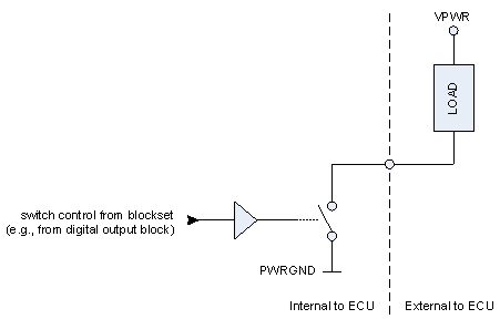
The ECU power arrangement is shown in Figure 4.1, “Switching arrangement for main power supply”.
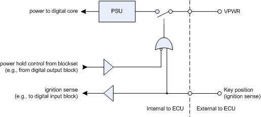
The ECU is powered up when the power supply pins (VPWR A10+A20+A30) and key position (ignition sense) input (pin A12) are asserted. The key position input (pin A12) can be read as a digital input.
This arrangement allows for the ECU application software to hold the ECU on after the external key position input is opened, allowing, for example, non-volatile memory processing to occur. For the ECU to hold power the internal DOT hold-PSU channel needs to be asserted. Setting this internal channel low will hold power when the key position input is opened, setting it high will allow the ECU to power off when the key position input is opened.
Note
When using the 'power hold' functionality, it is best to set the internal DOT hold-PSU channel low as soon as the external key position input (pin A12) is closed and only set high once all required shutdown tasks have completed.
Unlike some other ECUs, the M461-000 does provide an actuator supply.
Note
When using the high-side actuator output control, all loads controlled by a low-side drive output must be supplied by the high-side actuator output. If the system includes loads controlled by low-side drive outputs supplied by the high-side actuator output and others supplied directly from battery positive, there is a potential for a sneak path to provide power to some actuators even if the module is powered off. If it is desirable to connect loads controlled by low-side outputs directly to battery positive, then do not use the high-side actuator output to control power to other loads controlled by low-side outputs.
The ECU provides four external sensor power supplies (pins A8, A18, C8 and C18) and common sensor ground (pins A9, A19, C9 and C19).
The sensors supplies can be individually switched off to allow the application software to perform intrusive diagnostics on sensors. Each output is monitored by an internal analogue input channel which can be used to check for short circuits and measure the exact output voltage for use with ratio-metric sensors.
The output voltage is guaranteed to never reach full scale in normal operation, hence a full scale indication should be taken to indicate a suspected short to battery. The value read from the voltage monitor when the corresponding PSU is enabled should be interpreted as follows:
Table 4.1. Sensor supply monitor voltages
| Voltage | Meaning |
|---|---|
| > 4.97V | Output shorted to battery |
| 4.85V - 4.95V | Normal operation |
| < 4.85V | Output over-current or short to ground |
The value read from the common sensor ground voltage monitor should be interpreted as follows:
Table 4.2. Sensor ground monitor voltage
| Voltage | Meaning |
|---|---|
| 0mV - 20mV | Normal Operation |
| > 20mV | Output over current or short to battery |
The sensor ground feedback can also be used in normal operation by the application software to provide a precision ground reference for ratio-metric measurements.
The analogue inputs (pins A16, A22, A23, A24, A28, A32, A33, A34, C3, C4, C6, C13, C14, C16, C21, C22, C23, C24, C25, C31, C32, C33 and C35) sample voltage with varying resolution and range. See the pin information for more details. Some of the analogue inputs have additional characteristics, as detailed in the following sections.
Note
If any of the pins A1, A5, A7, A11, A15, A17, A21, A25, A31, A35, C5, C10, C15 and C20 are not being used as digital outputs then it is possible for them to be used as analogue inputs with a range of 0V to 39V, a loading of 41k to VGND and a filter of 104Hz. Providing the output transistor is switched off, the pin can be driven by an external source and pin's voltage monitor will reflect the actual voltage on the pin.
Note
Serial numbers 0544, 0591, 0594 through 0601, and 0606 do not have a bandwidth limiting filter installed on analogue inputs C3, C13, and C21. As a result, these inputs will not filter out high frequency noise and such noise may affect the input value.
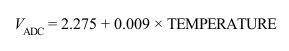
Although the ECU does not include thermocouple inputs, like some other ECUs, the M461-000 does retain the cold-junction temperature input which can be utilised as the internal temperature of the ECU.
The relationship between temperature and the ADC voltage (VADC) and ADC counts (CADC) for the internal temperature sensor is:
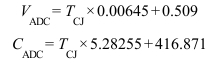
over a range of -40°C to +125°C.
The internal accelerometer channels (AIN accelerometer-x, AIN accelerometer-y and AIN accelerometer-z) have a zero point of 1.65V and give an output swing of 600mV/g. The relationship between acceleration and the ADC voltage (VADC) is:
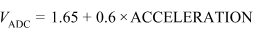
The full scale range of the accelerometer is ±2g so VADC will never reach 0V or 5V in normal operation.
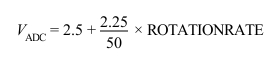
The internal gyroscope channels (AIN gyroscope-x, AIN gyroscope-y and AIN gyroscope-z) have a zero point of 2.5V and give an output swing of ±2.25V for rotation rates in the range ±50°/s. The relationship between rotation and the ADC voltage (VADC) is:
In addition to their analogue outputs, the gyroscopes have two self test signals (internal channels DOT gyro-self-test-1 and DOT gyro-self-test-2). Asserting these signals high introduces an offset to VADC for diagnostic purposes.
Asserting internal channel DOT gyro-self-test-1 high causes VADC to change -1.9V. Asserting internal channel DOT gyro-self-test-2 high causes an opposite change of +1.9V. The self-test response follows the viscosity temperature dependence of the package atmosphere, approximately 0.25%/°C.
Note
Asserting both self-test channels simultaneously is not damaging. Both are fairly closely matched (±5%), but asserting both high simultaneously may result in a small apparent null bias shift proportional to the degree of self-test mismatch.
The gyroscope devices provide a single temperature signal (internal channel AIN gyroscope-temperature. This signal may be used by the application software to compensate for drift of the gyroscopes. The relationship between temperature and the ADC voltage (VADC) for the gyroscope temperature sensor is:
over a range of -40°C to +125°C. Refer to the ADXRS614 data-sheet from Analog Devices for further information on temperature calibration.
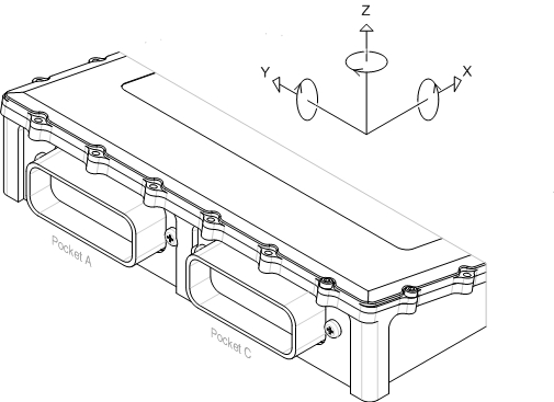
The accelerometer and gyroscope orientation is pictured below:
The inputs work on a voltage threshold. If the external pin is above the threshold voltage the input will be 0, if the external pin is below the threshold the input will be 1 (i.e. signal is inverted between the external pin and the software).
Note
The external signals are all low pass filtered to prevent signals of excessive frequency from tying up the target processor.
Note
If any of the pins A1, A5, A7, A11, A15, A17, A21, A25, A31, A35, C5, C10, C15 and C20 are not being used as digital outputs then it is possible for them to be used as digital inputs with a loading of 41k to VGND and no input filter. Providing the output transistor is switched off, the pin can be driven by an external source and the pin's digital monitor will reflect the actual state of the pin. The digital monitor signal is not inverted: low if <= 3.5V and high if >= 6.9V.
The digital outputs (pins A1, A5, A7, A11, A15, A17, A21, A25, A31, A35, C5, C10, C15 and C20) are low-side drivers. That is, the ECU switches the output pin to ground, the actuator is connected to the output pin and the battery.
Note
The underlying timer for the M461 I/O has a rate of 4MHz.
The low-side digital outputs contain internal monitoring circuitry that provides diagnostic information. However, as a consequence a small leakage current will flow through the actuator when the low-side output driver is turned off. Refer to Table 4.3, “Low-side digital output leakage current” for typical leakage currents at specified operating voltages.
Table 4.3. Low-side digital output leakage current
| Supply Voltage (V) | Typical Leakage Current (mA) |
|---|---|
| 12 | 0.400 |
| 24 | 0.800 |
The actual state of an output pin can be monitored using a corresponding internal digital monitor and internal analogue monitor channel. The digital monitor channel simply reflects the on or off state of the actual output. The analogue monitor channel measures the actual voltage at the pin after scaling.
The over-current trip state of an output pin can be monitored using a corresponding internal over-current monitor channel. In normal operation the internal over-current trip channel will be 1. If the output channel experiences an over-current, the output channel will be forced off by the ECU and the over-current trip channel will be set to 0.
The over-current trip latch can be cleared and the tripped outputs enabled by the pss_OvercurTripReset Simulink block or by calling the pss_overcur_trip_reset() C-API function.
Note
To help component heat dissipation and to help prevent component stress, the platform software ensures there is at least 50ms between each request to clear the over-current trip latches.
Some of the internal and external inputs and outputs are classed as serial. The connector pinout tables and internal channel tables above specify whether a pin or channel is serial or not.
When a serial input is read, the measurement reflects the value of the input taken last time the application task ended. I.e., the value of the input is delayed by one cycle of the task period. When a serial output is set, the driven state is updated at the end of the current application task. I.e., there is a delay between requesting a change in the output state, and the output state honoring that request.
The CAN buses (pins A37+A36 and C37+C36) are implemented using high-speed CAN transceivers. Each CAN bus has terminating resistors fitted. Fleet and developer ECUs support two CAN buses (see the pin details for more information).
The ECU supports different memory configurations for application, calibration and RAM sizes, some of which require external calibration RAM (see Section 4.18, “Memory — calibration capabilities”).
Table 4.4. Memory configurations supported
|
Configuration |
App size (KiB) |
Cal size (KiB) |
RAM size (KiB) |
External RAM required? |
Run-time
calibration supported? |
|---|---|---|---|---|---|
| A [a] | 512 | 256 | 64 | N | N |
| 512 | 256 | 64 | Y | Y | |
| B | 512 | 256 | 832 | Y | Y |
| C | 640 | 128 | 192 | Y | Y |
| D | 768 | 64 | 768 | Y | Y |
[a] If an OpenECU target that supports memory configuration is loaded with an application in which no such configuration has been specified, then configuration A will be used as the default. | |||||
The ECU supports non-volatile memory storage in Flash. Battery backed RAM is not supported.
The processor's Flash memory is split into small and large memory blocks. The application and calibration are stored in large blocks, whilst DTC information, freeze frames and so on are stored in small blocks.
The largest Flash block can take up to approximately 7.5 seconds to erase. This occurs in an environment where the Flash has been erased and programmed many times at its temperature extreme. The typical erase time is smaller, especially at ambient temperatures. Reprogramming an ECU (where many large blocks would be erased), or storing DTC information across power cycles, can therefore take some time. Users and applications should take this into consideration.
The minimum number of erase cycles is approximately 1,000 for large Flash blocks and 100,000 for small Flash blocks. This occurs in an environment where the Flash has been erased and programmed many times at its temperature extreme. The typical number of erase cycles is larger, especially at ambient temperatures.
The minimum data retention is approximately 5 years for blocks which have been erased less than 100,000 times, and approximately 20 years for blocks which have been erased less than 1,000 times.
The information about the Flash has been taken from Freescale's MPC5534 Microcontroller Data Sheet document, revision 4 (dated Mar 2008).
The ECU supports both offline calibration (where all of the ECU's calibration memory is reprogrammed whilst the application is stopped) and online calibration (where individual calibrations can be modified whilst the application runs). These calibration capabilities are supported through two ECU types:
Developer ECUs — Supports offline and online calibration Uses an external RAM device to map calibrations, normally stored in non-volatile memory, to RAM to support modifications of calibration whilst the application runs. This provides all of the processor's RAM for the application and platform library, whilst adding additional RAM to support calibration.
Fleet ECUs — Does not provide external RAM or the ability to calibrate whilst the application runs (offline calibration is still supported). These units are lower-cost and intended for fleet trials or production.
The ECU can run in one of two system modes: reprogramming mode and application mode. In reprogramming mode, the ECU can be reprogrammed with application software from a calibration tool. In application mode, the ECU runs the programmed application software. The ECU enters reprogramming mode either by measuring the external FEPS A2 pin at power up, or when attempting to reflash over CCP when the application is not inhibiting reflashing.
Table 4.5. System mode selection
| Voltage | System mode |
|---|---|
| > +17V | Enter reprogramming mode. If valid application software has previously been programmed, then use the CCP settings from that application, otherwise use the default CCP settings. |
| < -16V | Enter reprogramming mode. Use the default CCP settings. |
| Otherwise | Enter application mode if valid application software has previously been programmed, otherwise enter reprogramming mode. |
Note
The default CCP baud rate for the M461 is 250kbps.
The ECU has a dedicated external pin (A27) for flashing a lamp. The flash sequence represents a set of codes. Each code is a three digit number, where each digit is flashed a number of times equal to its value.
An example would be the flash sequence for code 113. The flash sequence is broken down into a series on marks, or on and off pulses as follows:
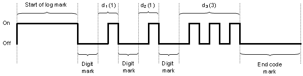
Each of the marks lasts for a specific duration:
Table 4.6. Flash code example
| Mark | Duration and meaning |
|---|---|
| Start of log mark | 3s — marks the start of the flash code list |
| Digit mark | 1s — marks the start of a digit |
| dn | ns — n digits, where the output is turned off for 0.5 second, then for 0.5 seconds, n times |
| End code mark | 3s — marks the end of a code (i.e., end of 3 digits) |
After the end code mark, the ECU will either flash the next code, or return to the start of the list and flash the first code. The ECU always has at least one code to flash.
Each code represents information about the ECU state. If there is no flash sequence, or a malformed flash sequence, then the ECU is malfunctioning. Otherwise, the flash sequence will represent one of the following codes:
Table 4.7. Flash codes
| Code | Meaning |
|---|---|
| 111 | In application mode — no other condition has been detected. |
| 112 | In reprogramming mode with the FEPS pin negative. |
| 113 | In reprogramming mode with the FEPS pin high. |
| 114 | In reprogramming mode via a FEPS-less reprogramming request. |
| 115 | In reprogramming mode because no valid application software exists. |
| 116 | In reprogramming mode due to FEPS pin electrical failure. |
| 117 | In reprogramming mode due to repeated reset during application mode. |
| 118 | In reprogramming mode due to failed application checksum tests. |
| 128 | In reprogramming mode due to failed memory check tests. |
| 119 | In reprogramming mode due to a FEPS-less ISO reprogramming request. |
| 121 | In reprogramming mode due to an unknown failure. |
| 123 | In reprogramming mode due to a watchdog reset. |
| 222 | In reprogramming mode due to the application not having a valid license. |
Developer units have the capability to accept calibration changes while the application software is running. Fleet units do not have this capability.
The ECU closely adheres to the IEEE-754 for floating point numbers.
When using Simulink, floating point Simulink models are supported — all calculations are performed using single-precision (even if the model uses double-precision, the ECU performs calculations using single-precision).
When using the C-API, floating point applications are supported — all calculations are performed using single or double precision, as determined by the application code (although double precision will incur some software overhead — see the compiler reference manual for further details).
The rounding mode is set to round-to-nearest. In some conditions, the ECU will not adhere to the IEEE-754 standard:
Table 4.8. Floating point conditions
| Condition | Result |
|---|---|
| Underflow | The result of a calculation underflow is ±0. The sign is based on the signs of the operands. |
| Overflow | The result of a calculation overflow is ±max where max is approximately 3.4 × 1038. The sign is based on the signs of the operands. |
| Divide by zero |
The ECU does not generate ±Inf, NaN or a denormalised number as the result of a calculation.
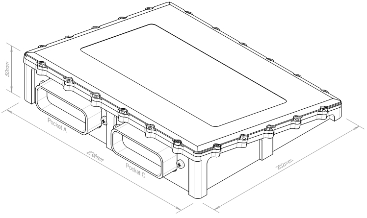
The ECU has the following dimensions:
If you have questions, or are experiencing issues with OpenECU please see the FAQ website:
- website
If you still have questions after searching through the FAQ, or want to discuss sales or proposals, you can contact main office:
- Tel
- +1 734 656 0140
- Fax
- +1 734 656 0141
during normal working hours (Mon to Fri, 0930 to 1700 EST).